Xem thông số kỹ thuật để biết chi tiết sản phẩm.

XC6SLX25T-3FG484I
Product Overview
Category
The XC6SLX25T-3FG484I belongs to the category of Field-Programmable Gate Arrays (FPGAs).
Use
FPGAs are integrated circuits that can be programmed after manufacturing, allowing for flexible and customizable digital logic designs. The XC6SLX25T-3FG484I is specifically designed for high-performance applications.
Characteristics
- High-performance FPGA with advanced features
- Offers a large number of programmable logic cells and built-in memory blocks
- Supports various I/O standards and interfaces
- Provides high-speed connectivity options
- Can be reprogrammed multiple times
Package
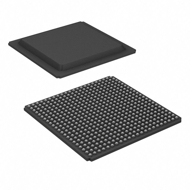
The XC6SLX25T-3FG484I comes in a FG484 package, which refers to a Fine-Pitch Ball Grid Array (BGA) package with 484 pins.
Essence
The essence of the XC6SLX25T-3FG484I lies in its ability to provide a versatile and customizable solution for complex digital logic designs.
Packaging/Quantity
The XC6SLX25T-3FG484I is typically packaged individually and is available in various quantities depending on the manufacturer's specifications.
Specifications
- Logic Cells: 24,576
- Block RAM: 1,080 Kb
- DSP Slices: 48
- Maximum Frequency: 550 MHz
- I/O Pins: 232
- Operating Voltage: 1.2V
- Operating Temperature Range: -40°C to 100°C
Detailed Pin Configuration
The XC6SLX25T-3FG484I has a total of 484 pins, each serving a specific purpose in the FPGA's functionality. A detailed pin configuration diagram can be found in the product datasheet provided by the manufacturer.
Functional Features
- High-performance programmable logic cells for complex digital designs
- Built-in memory blocks for efficient data storage and retrieval
- DSP slices for implementing signal processing algorithms
- Flexible I/O standards and interfaces for seamless integration with external devices
- Clock management resources for precise timing control
Advantages and Disadvantages
Advantages
- Flexibility: The XC6SLX25T-3FG484I allows for the customization of digital logic designs, making it suitable for a wide range of applications.
- Reconfigurability: The FPGA can be reprogrammed multiple times, enabling design iterations and updates without requiring hardware changes.
- High Performance: With a large number of logic cells and advanced features, the XC6SLX25T-3FG484I offers high-speed and efficient operation.
Disadvantages
- Complexity: Utilizing FPGAs requires expertise in digital design and programming, which may pose a challenge for beginners.
- Power Consumption: FPGAs tend to consume more power compared to fixed-function integrated circuits, especially when operating at high frequencies.
Working Principles
The XC6SLX25T-3FG484I operates based on the principles of configurable logic. It consists of an array of programmable logic cells interconnected through configurable routing resources. These logic cells can be programmed to implement various digital functions, allowing for the creation of complex digital systems.
Detailed Application Field Plans
The XC6SLX25T-3FG484I finds applications in various fields, including:
- Communications: Used in networking equipment, routers, and switches for high-speed data processing and protocol handling.
- Aerospace and Defense: Employed in radar systems, avionics, and military communication systems for their flexibility and performance.
- Industrial Automation: Utilized in control systems, robotics, and machine vision applications for real-time processing and control.
- Medical Devices: Integrated into medical imaging systems, patient monitoring devices, and diagnostic equipment for high-performance data processing.
Detailed and Complete Alternative Models
- XC6SLX25-2FGG484C
- XC6SLX25-3CSG324I
- XC6SLX25T-2FGG484I
- XC6SLX25T-2CSG324C
These alternative models offer similar functionality and performance to the XC6SLX25T-3FG484I and can be considered as alternatives based on specific project requirements.
Note: The above information is provided as a general overview. For detailed technical specifications and application-specific considerations, please refer to the manufacturer's datasheet and consult with experts in the field.
Liệt kê 10 câu hỏi và câu trả lời thường gặp liên quan đến ứng dụng XC6SLX25T-3FG484I trong giải pháp kỹ thuật
Sure! Here are 10 common questions and answers related to the application of XC6SLX25T-3FG484I in technical solutions:
Question: What is the XC6SLX25T-3FG484I?
Answer: The XC6SLX25T-3FG484I is a field-programmable gate array (FPGA) from Xilinx, which is commonly used in various technical solutions.Question: What are the key features of the XC6SLX25T-3FG484I?
Answer: Some key features of this FPGA include 25,920 logic cells, 36 DSP slices, 240KB block RAM, and support for various I/O standards.Question: What are the typical applications of the XC6SLX25T-3FG484I?
Answer: This FPGA is often used in applications such as industrial automation, telecommunications, medical devices, aerospace, and defense systems.Question: How can I program the XC6SLX25T-3FG484I?
Answer: You can program this FPGA using Xilinx's Vivado Design Suite or ISE Design Suite software tools.Question: What is the maximum operating frequency of the XC6SLX25T-3FG484I?
Answer: The maximum operating frequency of this FPGA depends on the specific design and implementation, but it can typically reach several hundred megahertz.Question: Can I interface the XC6SLX25T-3FG484I with other components or peripherals?
Answer: Yes, this FPGA supports various communication protocols such as SPI, I2C, UART, and Ethernet, allowing you to interface with other components or peripherals.Question: Does the XC6SLX25T-3FG484I support high-speed serial interfaces?
Answer: Yes, this FPGA supports high-speed serial interfaces such as PCIe, SATA, and USB, making it suitable for applications requiring fast data transfer.Question: What is the power consumption of the XC6SLX25T-3FG484I?
Answer: The power consumption of this FPGA depends on the specific design and utilization, but it typically ranges from a few watts to tens of watts.Question: Can I use the XC6SLX25T-3FG484I in a battery-powered application?
Answer: While it is possible to use this FPGA in a battery-powered application, the power consumption should be carefully considered to ensure optimal battery life.Question: Are there any development boards or evaluation kits available for the XC6SLX25T-3FG484I?
Answer: Yes, Xilinx offers various development boards and evaluation kits that include the XC6SLX25T-3FG484I, allowing you to quickly prototype and test your designs.
Please note that the answers provided here are general and may vary depending on the specific requirements and implementation of your technical solution.

