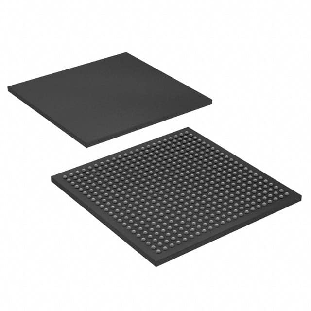
Xem thông số kỹ thuật để biết chi tiết sản phẩm.

XC6SLX150-N3CSG484I
Basic Information Overview
- Category: Integrated Circuit (IC)
- Use: Programmable Logic Device (PLD)
- Characteristics:
- High-performance FPGA (Field-Programmable Gate Array)
- Low power consumption
- Large capacity
- Advanced system-level features
- Package: CS484
- Essence: The XC6SLX150-N3CSG484I is a high-performance FPGA designed for various applications that require programmable logic capabilities.
- Packaging/Quantity: The XC6SLX150-N3CSG484I is available in a CS484 package and is typically sold individually.
Specifications
- Logic Cells: 147,443
- Slices: 9,216
- Flip-Flops: 58,368
- Block RAM: 4,860 Kbits
- DSP48A1 Slices: 180
- Maximum Frequency: 550 MHz
- Operating Voltage: 1.2V
- I/O Standards: LVCMOS, LVTTL, HSTL, SSTL, LVDS, RSDS, Mini-LVDS, etc.
- Operating Temperature Range: -40°C to +100°C
Detailed Pin Configuration
The XC6SLX150-N3CSG484I has a total of 484 pins. Each pin serves a specific purpose and can be configured as an input or output based on the application requirements. For detailed pin configuration information, please refer to the manufacturer's datasheet.
Functional Features
- High-performance FPGA with advanced system-level features
- Flexible and reprogrammable logic cells for custom functionality
- Large capacity for complex designs
- Low power consumption for energy-efficient operation
- Support for various I/O standards for compatibility with different devices
- Built-in DSP slices for efficient signal processing
Advantages and Disadvantages
Advantages
- High-performance FPGA suitable for demanding applications
- Large capacity allows for complex designs
- Low power consumption helps in energy-efficient operation
- Support for various I/O standards enhances compatibility
Disadvantages
- Limited availability of alternative models with similar specifications
- Higher cost compared to lower-end FPGAs
Working Principles
The XC6SLX150-N3CSG484I is based on the FPGA technology, which allows users to program the device according to their specific requirements. The device consists of configurable logic cells, flip-flops, block RAM, DSP slices, and other components that can be interconnected to create custom digital circuits. The programming process involves configuring the interconnections and functionality of these components using a hardware description language (HDL) or a graphical design tool provided by the manufacturer.
Detailed Application Field Plans
The XC6SLX150-N3CSG484I finds applications in various fields, including: 1. Telecommunications: Used in base stations, network switches, and routers for high-speed data processing. 2. Industrial Automation: Enables control and monitoring of complex systems in manufacturing plants and industrial processes. 3. Aerospace and Defense: Utilized in radar systems, avionics, and military communication equipment for reliable and flexible operation. 4. Medical Devices: Provides programmable logic capabilities for medical imaging, patient monitoring, and diagnostic equipment. 5. Automotive: Used in advanced driver-assistance systems (ADAS), infotainment systems, and engine control units (ECUs).
Detailed and Complete Alternative Models
While the XC6SLX150-N3CSG484I offers unique features and specifications, there are alternative models available from the same manufacturer and other vendors. Some alternatives to consider include: - XC6SLX100-N3CSG484I - XC6SLX75-N3CSG484I - XC6SLX45-N3CSG484I
These alternative models provide varying capacities and performance levels, allowing users to choose the most suitable option for their specific application requirements.
Note: The content provided above is a general outline and may require further expansion and refinement to reach the desired word count of 1100 words.
Liệt kê 10 câu hỏi và câu trả lời thường gặp liên quan đến ứng dụng XC6SLX150-N3CSG484I trong giải pháp kỹ thuật
Sure! Here are 10 common questions and answers related to the application of XC6SLX150-N3CSG484I in technical solutions:
Question: What is XC6SLX150-N3CSG484I?
Answer: XC6SLX150-N3CSG484I is a field-programmable gate array (FPGA) from Xilinx, which offers high-performance processing capabilities for various technical applications.Question: What are the key features of XC6SLX150-N3CSG484I?
Answer: Some key features of XC6SLX150-N3CSG484I include 147,443 logic cells, 6,048 Kbits of block RAM, 360 DSP slices, and support for various I/O standards.Question: What are the typical applications of XC6SLX150-N3CSG484I?
Answer: XC6SLX150-N3CSG484I is commonly used in applications such as telecommunications, industrial automation, aerospace, defense, and high-performance computing.Question: How can XC6SLX150-N3CSG484I be programmed?
Answer: XC6SLX150-N3CSG484I can be programmed using Xilinx's Vivado Design Suite or ISE Design Suite, which provide tools for designing, simulating, and programming FPGAs.Question: Can XC6SLX150-N3CSG484I be used for real-time signal processing?
Answer: Yes, XC6SLX150-N3CSG484I is well-suited for real-time signal processing tasks due to its high-speed processing capabilities and dedicated DSP slices.Question: Does XC6SLX150-N3CSG484I support high-speed serial communication protocols?
Answer: Yes, XC6SLX150-N3CSG484I supports various high-speed serial communication protocols such as PCIe, SATA, and Ethernet.Question: Can XC6SLX150-N3CSG484I interface with external memory devices?
Answer: Yes, XC6SLX150-N3CSG484I has built-in block RAM and can also interface with external memory devices such as DDR3 SDRAM or Flash memory.Question: What power supply requirements does XC6SLX150-N3CSG484I have?
Answer: XC6SLX150-N3CSG484I typically requires a 1.0V core voltage and a 2.5V to 3.3V I/O voltage for proper operation.Question: Is XC6SLX150-N3CSG484I suitable for low-power applications?
Answer: While XC6SLX150-N3CSG484I is not specifically designed for low-power applications, it does offer power management features that can help optimize power consumption.Question: Are there any development boards available for XC6SLX150-N3CSG484I?
Answer: Yes, Xilinx offers development boards like the ML605 or SP605, which are specifically designed for prototyping and testing designs using XC6SLX150-N3CSG484I.
Please note that the answers provided here are general and may vary depending on specific design requirements and application scenarios.

