

Xem thông số kỹ thuật để biết chi tiết sản phẩm.
SN74LVU04ARGYRG4
Product Overview
- Category: Integrated Circuit (IC)
- Use: Inverting Hex Buffer/Driver
- Characteristics:
- Low-voltage operation
- High-speed performance
- Wide operating temperature range
- RoHS compliant
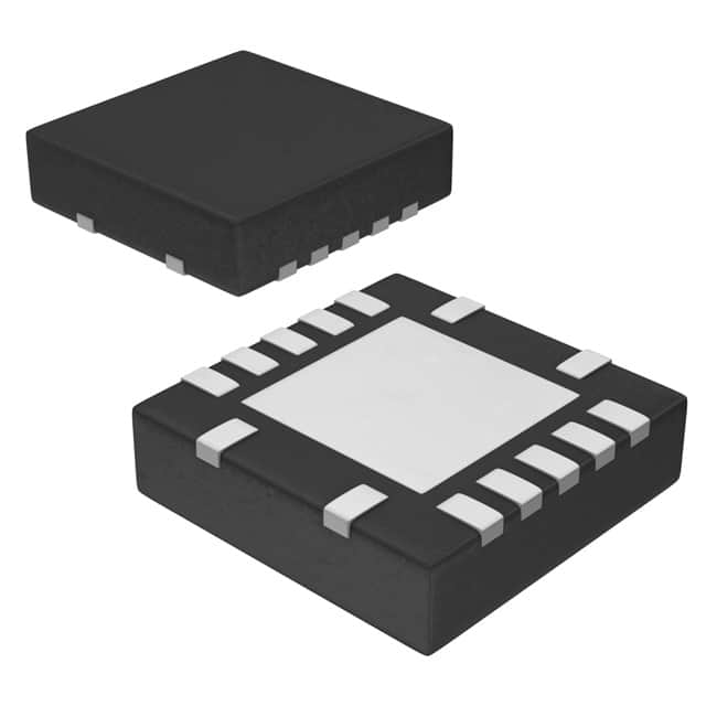
- Package: VQFN-20
- Essence: Hex inverter gate
- Packaging/Quantity: Tape and Reel, 2500 units per reel
Specifications
- Supply Voltage Range: 1.65V to 5.5V
- Input Voltage Range: 0V to VCC
- Output Voltage Range: 0V to VCC
- Maximum Operating Frequency: 50MHz
- Propagation Delay Time: 6.2ns (typical)
- Input Capacitance: 3pF (typical)
- Output Current: ±8mA
- Operating Temperature Range: -40°C to +125°C
Detailed Pin Configuration
The SN74LVU04ARGYRG4 has a VQFN-20 package with the following pin configuration:
__    __
   A1 | 1    20 | VCC
   A2 | 2    19 | Y1
   B1 | 3    18 | A6
   B2 | 4    17 | Y2
   A3 | 5    16 | A5
   A4 | 6    15 | Y3
   GND| 7    14 | A7
   Y4 | 8    13 | Y6
   AY | 9    12 | AY
   Y5 |10    11 | Y7
       ‾‾    ‾‾
Functional Features
- Hex inverter gate: The SN74LVU04ARGYRG4 consists of six independent inverter gates, each capable of converting a high-level input signal to its complementary low-level output.
- Low-voltage operation: It operates at a supply voltage range of 1.65V to 5.5V, making it suitable for various low-power applications.
- High-speed performance: With a maximum operating frequency of 50MHz and a propagation delay time of 6.2ns (typical), it ensures efficient signal processing.
- Wide operating temperature range: It can operate reliably in temperatures ranging from -40°C to +125°C.
- RoHS compliant: The product is compliant with the Restriction of Hazardous Substances directive, ensuring environmental safety.
Advantages and Disadvantages
Advantages: - Low-voltage operation allows for compatibility with a wide range of systems. - High-speed performance enables fast signal processing. - Wide operating temperature range ensures reliability in extreme conditions. - RoHS compliance promotes environmental sustainability.
Disadvantages: - Limited output current may restrict usage in certain applications requiring higher current levels. - Propagation delay time may affect real-time applications that demand instantaneous response.
Working Principles
The SN74LVU04ARGYRG4 operates based on the principles of digital logic. Each inverter gate within the IC receives an input signal and produces the logical complement of that input as the output. The low-voltage operation allows for compatibility with modern low-power devices, while the high-speed performance ensures efficient signal processing.
Detailed Application Field Plans
The SN74LVU04ARGYRG4 finds applications in various fields, including:
- Communication Systems: It can be used for signal inversion and buffering in communication systems, ensuring reliable data transmission.
- Industrial Automation: The IC can be employed in control systems, motor drives, and robotics, providing signal conditioning and level shifting capabilities.
- Automotive Electronics: It finds use in automotive applications such as engine control units, infotainment systems, and lighting control, ensuring accurate signal processing.
- Consumer Electronics: The IC can be utilized in devices like smartphones, tablets, and gaming consoles for signal inversion and level shifting.
Detailed and Complete Alternative Models
- SN74LVC04ARGYRG4: Similar to SN74LVU04ARGYRG4, but operates at a higher voltage range of 1.65V to 3.6V.
- SN74AHC04RGYR: An alternative model with similar functionality, but operates at a wider voltage range of 2V to 5.5V.
- SN74HCU04ARGYRG4: Another alternative model that offers enhanced noise immunity and operates at a voltage range of 2V to 6V.
These alternative models provide options based on specific voltage requirements and additional features needed for different applications.
In conclusion, the SN74LVU04ARGYRG4 is a versatile hex inverter gate IC that operates at low voltages, offers high-speed performance
Liệt kê 10 câu hỏi và câu trả lời thường gặp liên quan đến ứng dụng SN74LVU04ARGYRG4 trong giải pháp kỹ thuật
Sure! Here are 10 common questions and answers related to the application of SN74LVU04ARGYRG4 in technical solutions:
Q: What is SN74LVU04ARGYRG4? A: SN74LVU04ARGYRG4 is a hex inverter IC (integrated circuit) manufactured by Texas Instruments.
Q: What is the purpose of SN74LVU04ARGYRG4? A: SN74LVU04ARGYRG4 is used to invert logic signals, converting high voltage levels to low and vice versa.
Q: What is the operating voltage range of SN74LVU04ARGYRG4? A: The operating voltage range of SN74LVU04ARGYRG4 is typically between 1.65V and 5.5V.
Q: How many inverters are there in SN74LVU04ARGYRG4? A: SN74LVU04ARGYRG4 contains six independent inverters in a single package.
Q: What is the maximum output current of SN74LVU04ARGYRG4? A: The maximum output current of SN74LVU04ARGYRG4 is typically around 8mA.
Q: Can SN74LVU04ARGYRG4 be used with both CMOS and TTL logic levels? A: Yes, SN74LVU04ARGYRG4 is compatible with both CMOS and TTL logic levels.
Q: What is the propagation delay of SN74LVU04ARGYRG4? A: The propagation delay of SN74LVU04ARGYRG4 is typically around 5 ns.
Q: Is SN74LVU04ARGYRG4 suitable for high-speed applications? A: Yes, SN74LVU04ARGYRG4 is designed for high-speed operation and can be used in various high-frequency applications.
Q: Can SN74LVU04ARGYRG4 be used in both digital and analog circuits? A: SN74LVU04ARGYRG4 is primarily designed for digital logic applications but can also be used in certain analog circuits.
Q: What are some common applications of SN74LVU04ARGYRG4? A: SN74LVU04ARGYRG4 is commonly used in signal inversion, level shifting, clock buffering, and general-purpose logic gate applications.
Please note that the answers provided here are general and may vary depending on specific use cases and requirements.