

Xem thông số kỹ thuật để biết chi tiết sản phẩm.
SN74LVU04ADGVRE4
Product Overview
- Category: Integrated Circuit
- Use: Logic Gate Inverter
- Characteristics: Low-voltage, Ultra-low power consumption
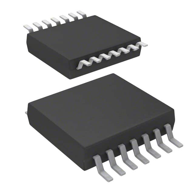
- Package: VSON (Very Small Outline No-Lead)
- Essence: Hex Inverter
- Packaging/Quantity: Tape and Reel, 2500 units per reel
Specifications
- Supply Voltage Range: 1.65V to 5.5V
- Input Voltage Range: 0V to VCC
- Output Voltage Range: 0V to VCC
- Operating Temperature Range: -40°C to +125°C
- Propagation Delay Time: 6.2ns (typical) at 3.3V
- Quiescent Current: 10μA (maximum) at 3.3V
Detailed Pin Configuration
The SN74LVU04ADGVRE4 has a total of 14 pins. The pin configuration is as follows:
- GND (Ground)
- A1 (Input A)
- Y1 (Output Y)
- A2 (Input A)
- Y2 (Output Y)
- A3 (Input A)
- Y3 (Output Y)
- VCC (Power Supply)
- A4 (Input A)
- Y4 (Output Y)
- A5 (Input A)
- Y5 (Output Y)
- A6 (Input A)
- Y6 (Output Y)
Functional Features
- Hex inverter with six independent inverters
- High-speed operation with low power consumption
- Wide supply voltage range allows compatibility with various systems
- Schmitt-trigger inputs for noise immunity
- Balanced propagation delays ensure accurate signal transmission
Advantages and Disadvantages
Advantages
- Low-voltage operation enables energy-efficient designs
- Ultra-low power consumption prolongs battery life
- Schmitt-trigger inputs provide noise immunity
- Compact VSON package saves board space
Disadvantages
- Limited number of inverters (six in total)
- Not suitable for high-speed applications
Working Principles
The SN74LVU04ADGVRE4 is a hex inverter integrated circuit. It consists of six independent inverters, each capable of converting a logic level input signal to its complemented output. The device operates at low voltages, making it suitable for battery-powered applications. The Schmitt-trigger inputs ensure reliable operation by providing noise immunity. The balanced propagation delays guarantee accurate signal transmission.
Detailed Application Field Plans
The SN74LVU04ADGVRE4 finds applications in various fields, including:
- Consumer Electronics: Used in smartphones, tablets, and portable devices for voltage level conversion and signal inversion.
- Industrial Automation: Employed in control systems, PLCs, and robotics for logic signal processing and interfacing.
- Automotive Electronics: Integrated into automotive modules and ECUs for signal conditioning and data communication.
- Communication Systems: Utilized in networking equipment, routers, and switches for signal inversion and buffering.
- Medical Devices: Incorporated into medical instruments and diagnostic equipment for signal amplification and conversion.
Detailed and Complete Alternative Models
- SN74LVC04A: Similar hex inverter with 5V tolerant inputs and outputs.
- SN74AHC04: Hex inverter with higher speed and wider operating temperature range.
- SN74LV14A: Hex Schmitt-trigger inverter with hysteresis for improved noise immunity.
- SN74HCU04: Hex unbuffered inverter with high-speed operation and low power consumption.
These alternative models offer similar functionality to the SN74LVU04ADGVRE4 but may have different specifications or additional features.
In conclusion, the SN74LVU04ADGVRE4 is a low-voltage hex inverter integrated circuit with six independent inverters. It operates at ultra-low power consumption and is housed in a compact VSON package. The device finds applications in various fields, including consumer electronics, industrial automation, automotive electronics, communication systems, and medical devices. Alternative models with similar functionality are available for specific design requirements.
Liệt kê 10 câu hỏi và câu trả lời thường gặp liên quan đến ứng dụng SN74LVU04ADGVRE4 trong giải pháp kỹ thuật
Sure! Here are 10 common questions and answers related to the application of SN74LVU04ADGVRE4 in technical solutions:
Q: What is SN74LVU04ADGVRE4? A: SN74LVU04ADGVRE4 is a hex inverter IC (integrated circuit) that provides six independent inverters with Schmitt-trigger inputs.
Q: What is the operating voltage range for SN74LVU04ADGVRE4? A: The operating voltage range for SN74LVU04ADGVRE4 is from 1.65V to 5.5V.
Q: What is the maximum output current of SN74LVU04ADGVRE4? A: The maximum output current of SN74LVU04ADGVRE4 is typically 8mA.
Q: Can SN74LVU04ADGVRE4 be used in both digital and analog applications? A: No, SN74LVU04ADGVRE4 is primarily designed for digital applications and may not be suitable for analog applications.
Q: What is the typical propagation delay of SN74LVU04ADGVRE4? A: The typical propagation delay of SN74LVU04ADGVRE4 is around 6 ns.
Q: Can SN74LVU04ADGVRE4 handle high-speed signals? A: Yes, SN74LVU04ADGVRE4 is capable of handling high-speed signals due to its Schmitt-trigger inputs.
Q: Is SN74LVU04ADGVRE4 compatible with TTL (Transistor-Transistor Logic) inputs? A: Yes, SN74LVU04ADGVRE4 is compatible with TTL inputs as it has TTL-compatible input thresholds.
Q: Can SN74LVU04ADGVRE4 be used in automotive applications? A: Yes, SN74LVU04ADGVRE4 is qualified for automotive applications and meets the AEC-Q100 standard.
Q: What is the package type of SN74LVU04ADGVRE4? A: SN74LVU04ADGVRE4 comes in a small VSSOP-14 package.
Q: Are there any recommended decoupling capacitors for SN74LVU04ADGVRE4? A: It is generally recommended to use a 0.1µF ceramic capacitor placed close to the power supply pins of SN74LVU04ADGVRE4 for proper decoupling.
Please note that these answers are general and may vary depending on specific application requirements.