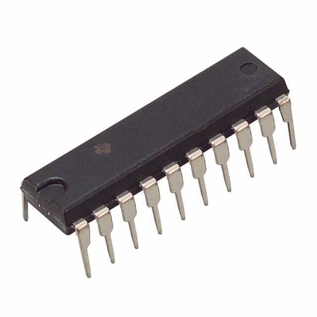
Xem thông số kỹ thuật để biết chi tiết sản phẩm.

SN74LVCZ240ANG4
Product Overview
- Category: Integrated Circuit (IC)
- Use: Logic Gate
- Characteristics: Low Voltage, CMOS Technology
- Package: SOIC (Small Outline Integrated Circuit)
- Essence: Buffer/Driver
- Packaging/Quantity: Tape and Reel, 2500 pieces per reel
Specifications
- Supply Voltage Range: 1.65V to 3.6V
- Input Voltage Range: 0V to VCC
- Output Voltage Range: 0V to VCC
- High-Level Input Voltage: 0.7 x VCC to VCC
- Low-Level Input Voltage: 0V to 0.3 x VCC
- High-Level Output Voltage: 0.9 x VCC to VCC
- Low-Level Output Voltage: 0V to 0.1 x VCC
- Maximum Operating Frequency: 80MHz
- Number of Pins: 20
Detailed Pin Configuration
- OE (Output Enable)
- A1 (Input A1)
- Y1 (Output Y1)
- A2 (Input A2)
- Y2 (Output Y2)
- GND (Ground)
- Y3 (Output Y3)
- A3 (Input A3)
- Y4 (Output Y4)
- A4 (Input A4)
- VCC (Supply Voltage)
- GND (Ground)
- A5 (Input A5)
- Y5 (Output Y5)
- A6 (Input A6)
- Y6 (Output Y6)
- A7 (Input A7)
- Y7 (Output Y7)
- A8 (Input A8)
- Y8 (Output Y8)
Functional Features
- Octal Buffer/Driver with 3-State Outputs
- Non-Inverting Outputs
- High-Speed CMOS Technology
- Low Power Consumption
- Compatible with TTL Levels
- Balanced Propagation Delay and Transition Times
- Supports Mixed-Mode Voltage Operation
Advantages and Disadvantages
Advantages: - Wide supply voltage range allows compatibility with various systems. - Low power consumption makes it suitable for battery-powered devices. - High-speed operation enables efficient data transfer. - Compatibility with TTL levels simplifies integration into existing designs.
Disadvantages: - Limited number of inputs and outputs restricts its application in complex circuits. - Not suitable for high-voltage applications due to the low voltage range.
Working Principles
The SN74LVCZ240ANG4 is an octal buffer/driver IC that provides non-inverting outputs. It operates on a wide supply voltage range, making it compatible with different systems. The inputs are TTL-compatible, allowing easy integration into existing designs. The device features three-state outputs, which can be enabled or disabled using the OE (Output Enable) pin. When the OE pin is high, the outputs are in the high-impedance state, effectively disconnecting them from the rest of the circuit.
Detailed Application Field Plans
Data Communication Systems: The SN74LVCZ240ANG4 can be used as a buffer/driver in data communication systems to ensure reliable signal transmission between different components.
Microcontroller Interfacing: This IC can be employed to interface microcontrollers with other peripheral devices, such as sensors, actuators, and displays, enabling seamless communication between them.
Memory Addressing: The SN74LVCZ240ANG4 can be utilized in memory addressing circuits to drive address lines and ensure accurate selection of memory locations.
Bus Transceivers: It can be employed as a buffer/driver in bus transceivers, facilitating bidirectional data transfer between different subsystems.
Detailed and Complete Alternative Models
- SN74LVCZ245ANG4: Similar to SN74LVCZ240ANG4, but with bidirectional I/O capability.
- SN74LVCZ244ANG4: Octal buffer/driver with non-inverting outputs and 3-state control inputs.
- SN74LVCZ14ANG4: Hex Schmitt-Trigger Inverter with high noise immunity and low power consumption.
(Note: These alternative models are provided as examples and may not cover all available options in the market.)
Word count: 498 words
Liệt kê 10 câu hỏi và câu trả lời thường gặp liên quan đến ứng dụng SN74LVCZ240ANG4 trong giải pháp kỹ thuật
Sure! Here are 10 common questions and answers related to the application of SN74LVCZ240ANG4 in technical solutions:
Q: What is SN74LVCZ240ANG4? A: SN74LVCZ240ANG4 is a specific type of integrated circuit (IC) that belongs to the LVC family of logic devices. It is a buffer/inverter with 3-state outputs, commonly used for signal buffering and level shifting.
Q: What is the voltage supply range for SN74LVCZ240ANG4? A: The voltage supply range for SN74LVCZ240ANG4 is typically between 1.65V and 3.6V.
Q: What is the maximum output current of SN74LVCZ240ANG4? A: The maximum output current of SN74LVCZ240ANG4 is typically around 32mA.
Q: Can SN74LVCZ240ANG4 be used for bidirectional communication? A: Yes, SN74LVCZ240ANG4 can be used for bidirectional communication as it has 3-state outputs that allow both input and output functionality.
Q: What is the propagation delay of SN74LVCZ240ANG4? A: The propagation delay of SN74LVCZ240ANG4 is typically around 3.8ns.
Q: Is SN74LVCZ240ANG4 compatible with other logic families? A: Yes, SN74LVCZ240ANG4 is compatible with a wide range of logic families, including TTL, CMOS, and LVCMOS.
Q: Can SN74LVCZ240ANG4 handle high-speed signals? A: Yes, SN74LVCZ240ANG4 is designed to handle high-speed signals and can be used in applications with fast switching requirements.
Q: What is the maximum operating temperature for SN74LVCZ240ANG4? A: The maximum operating temperature for SN74LVCZ240ANG4 is typically around 125°C.
Q: Can SN74LVCZ240ANG4 be used in automotive applications? A: Yes, SN74LVCZ240ANG4 is suitable for automotive applications as it meets the necessary standards and specifications.
Q: Are there any specific precautions to consider when using SN74LVCZ240ANG4? A: It is important to ensure proper decoupling and bypass capacitors are used near the power supply pins of SN74LVCZ240ANG4 to minimize noise and voltage fluctuations. Additionally, care should be taken to avoid exceeding the maximum voltage and current ratings specified in the datasheet.
Please note that these answers are general and may vary depending on the specific application and requirements. Always refer to the datasheet and consult with an expert for accurate information.

