

Xem thông số kỹ thuật để biết chi tiết sản phẩm.
SN74LVC827ANSRG4
Product Overview
Category
SN74LVC827ANSRG4 belongs to the category of integrated circuits (ICs).
Use
This IC is commonly used in digital logic applications for data storage and manipulation.
Characteristics
- Low-voltage CMOS technology
- High-speed operation
- Wide operating voltage range
- 3-state outputs
- Schmitt-trigger inputs
- ESD protection
Package
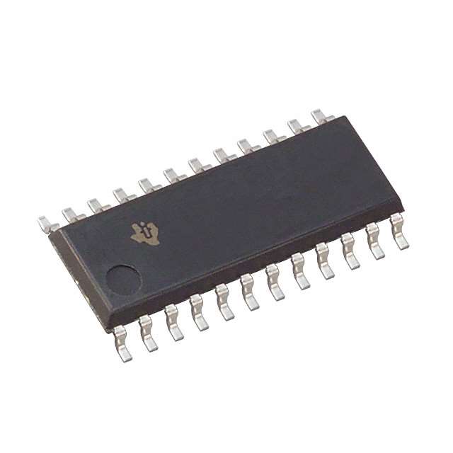
SN74LVC827ANSRG4 is available in a small-outline package (SOIC) with a surface-mount form factor.
Essence
The essence of SN74LVC827ANSRG4 lies in its ability to provide efficient and reliable digital logic functions, enabling data processing and storage in various electronic systems.
Packaging/Quantity
SN74LVC827ANSRG4 is typically packaged in reels or tubes, with a quantity of 2500 units per reel/tube.
Specifications
- Supply Voltage: 1.65V to 5.5V
- Input Voltage: -0.5V to VCC + 0.5V
- Output Voltage: -0.5V to VCC + 0.5V
- Operating Temperature Range: -40°C to 85°C
- Logic Family: LVC
- Number of Inputs: 10
- Number of Outputs: 10
- Propagation Delay: 2.9ns (typical)
Detailed Pin Configuration
The pin configuration of SN74LVC827ANSRG4 is as follows:
+-------------------+
   A1  |1                20| VCC
   B1  |2                19| Y1
   A2  |3                18| B2
   B2  |4                17| A3
   GND |5                16| B3
   Y2  |6                15| A4
   B4  |7                14| G1
   A4  |8                13| Y3
   G2  |9                12| B3
   Y3  |10               11| A3
       +-------------------+
Functional Features
- 10-bit buffer/line driver with 3-state outputs
- Non-inverting outputs
- High-speed operation
- Schmitt-trigger inputs for noise immunity
- ESD protection to prevent damage from electrostatic discharge
Advantages and Disadvantages
Advantages
- Low-voltage operation allows compatibility with a wide range of systems
- High-speed operation enables efficient data processing
- 3-state outputs provide flexibility in connecting multiple devices
- Schmitt-trigger inputs enhance noise immunity, ensuring reliable operation
- ESD protection safeguards the IC from electrostatic discharge damage
Disadvantages
- Limited number of inputs and outputs may restrict its application in complex systems
- Propagation delay of 2.9ns may not be suitable for ultra-high-speed applications
Working Principles
SN74LVC827ANSRG4 operates based on CMOS technology, utilizing transistors to implement digital logic functions. It acts as a buffer/line driver, receiving input signals and providing non-inverted output signals. The Schmitt-trigger inputs ensure reliable signal detection by reducing the impact of noise. The 3-state outputs allow multiple devices to share a common bus without interference.
Detailed Application Field Plans
SN74LVC827ANSRG4 finds applications in various fields, including: 1. Microcontrollers and microprocessors 2. Data storage systems 3. Communication equipment 4. Industrial automation 5. Automotive electronics
In microcontrollers and microprocessors, SN74LVC827ANSRG4 can be used for data buffering and signal conditioning. In data storage systems, it can facilitate data transfer between memory modules and processors. Communication equipment can benefit from its ability to drive signals over long distances. Industrial automation applications may utilize this IC for controlling and monitoring digital signals. Automotive electronics can employ SN74LVC827ANSRG4 for various digital logic functions.
Detailed and Complete Alternative Models
Some alternative models that offer similar functionality to SN74LVC827ANSRG4 are: 1. SN74LVC827ADGVR 2. SN74LVC827APW 3. SN74LVC827ADBR 4. SN74LVC827APWR 5. SN74LVC827ADGVRG4
These alternatives provide comparable features and can be considered based on specific requirements and availability.
Word count: 530 words
Liệt kê 10 câu hỏi và câu trả lời thường gặp liên quan đến ứng dụng SN74LVC827ANSRG4 trong giải pháp kỹ thuật
Sure! Here are 10 common questions and answers related to the application of SN74LVC827ANSRG4:
Q: What is SN74LVC827ANSRG4? A: SN74LVC827ANSRG4 is a quadruple bus buffer gate with 3-state outputs, designed for voltage level translation between different logic families.
Q: What is the operating voltage range of SN74LVC827ANSRG4? A: SN74LVC827ANSRG4 operates within a voltage range of 1.65V to 5.5V.
Q: Can SN74LVC827ANSRG4 be used as a bidirectional level shifter? A: No, SN74LVC827ANSRG4 is unidirectional and can only perform voltage level translation in one direction.
Q: What is the maximum data rate supported by SN74LVC827ANSRG4? A: SN74LVC827ANSRG4 supports a maximum data rate of 100 MHz.
Q: How many channels does SN74LVC827ANSRG4 have? A: SN74LVC827ANSRG4 has four independent channels.
Q: Can SN74LVC827ANSRG4 handle high-speed signals? A: Yes, SN74LVC827ANSRG4 is designed to handle high-speed signals with minimal propagation delay.
Q: What is the output drive strength of SN74LVC827ANSRG4? A: SN74LVC827ANSRG4 has a typical output drive strength of ±24 mA.
Q: Is SN74LVC827ANSRG4 compatible with both TTL and CMOS logic levels? A: Yes, SN74LVC827ANSRG4 is compatible with both TTL and CMOS logic levels.
Q: Can SN74LVC827ANSRG4 be used in automotive applications? A: Yes, SN74LVC827ANSRG4 is qualified for automotive applications and meets the necessary standards.
Q: What is the package type of SN74LVC827ANSRG4? A: SN74LVC827ANSRG4 is available in a 20-pin small-outline integrated circuit (SOIC) package.
Please note that these answers are general and may vary depending on the specific datasheet and application requirements.