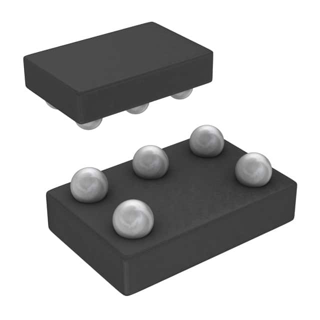
Xem thông số kỹ thuật để biết chi tiết sản phẩm.

SN74LVC1G240YZPR
Product Overview
- Category: Integrated Circuit
- Use: Logic Gate
- Characteristics: Single Buffer/Driver, Non-Inverting, 3-State Output
- Package: SOT-23-5
- Essence: Low-Voltage CMOS Logic
- Packaging/Quantity: Tape and Reel, 3000 pieces per reel
Specifications
- Supply Voltage Range: 1.65V to 5.5V
- Input Voltage Range: 0V to VCC
- Output Voltage Range: 0V to VCC
- Maximum Operating Frequency: 80 MHz
- Propagation Delay: 4.2 ns (typical)
- Output Drive Capability: ±24 mA
- Operating Temperature Range: -40°C to +85°C
Detailed Pin Configuration
The SN74LVC1G240YZPR has a total of 5 pins:
- GND (Ground): Connected to the ground reference of the circuit.
- VCC (Supply Voltage): Connected to the positive supply voltage.
- A (Input): Input pin for the logic signal.
- Y (Output): Output pin for the logic signal.
- OE (Output Enable): Control pin to enable/disable the output.
Functional Features
- Single buffer/driver with non-inverting 3-state output.
- Provides buffering and level shifting capabilities.
- Allows multiple devices to be connected together without bus contention.
- Supports bidirectional communication between different voltage domains.
- High-speed operation with low power consumption.
- Schmitt-trigger input allows for better noise immunity.
Advantages and Disadvantages
Advantages: - Small package size enables space-saving designs. - Wide supply voltage range allows compatibility with various systems. - 3-state output facilitates bus sharing in multi-device applications. - Low power consumption extends battery life in portable devices. - Schmitt-trigger input enhances noise immunity.
Disadvantages: - Limited output drive capability may restrict use in high-current applications. - Single buffer/driver limits the number of outputs per device. - Propagation delay may affect timing-sensitive applications.
Working Principles
The SN74LVC1G240YZPR is a low-voltage CMOS logic gate that operates as a single buffer/driver with a non-inverting 3-state output. It is designed to provide buffering and level shifting capabilities for digital signals. The device allows bidirectional communication between different voltage domains and supports bus sharing in multi-device applications.
The input signal is received at pin A, which is then processed by the internal circuitry. The output signal is available at pin Y. The OE (Output Enable) pin controls the output state, enabling or disabling the output. When the OE pin is high, the output is enabled, and when it is low, the output is disabled (high impedance state).
The SN74LVC1G240YZPR operates within a wide supply voltage range of 1.65V to 5.5V, making it compatible with various systems. It offers high-speed operation with low power consumption, making it suitable for battery-powered devices. The Schmitt-trigger input provides better noise immunity by reducing the effects of input signal noise.
Detailed Application Field Plans
The SN74LVC1G240YZPR can be used in various applications, including but not limited to:
- Microcontrollers and microprocessors
- Communication systems
- Industrial automation
- Automotive electronics
- Consumer electronics
- Portable devices
- Sensor interfaces
- Power management systems
- Medical equipment
- Internet of Things (IoT) devices
Detailed and Complete Alternative Models
- SN74LVC1G07: Single Buffer/Driver, Open-Drain Output
- SN74LVC1G17: Single Buffer/Driver, Schmitt-Trigger Input
- SN74LVC1G125: Single Bus Buffer Gate, 3-State Output
- SN74LVC1G32: Single OR Gate, 3-State Output
- SN74LVC1G86: Single XOR Gate, 3-State Output
These alternative models offer similar functionality and can be considered as alternatives to the SN74LVC1G240YZPR based on specific requirements and design constraints.
Word count: 537 words
Liệt kê 10 câu hỏi và câu trả lời thường gặp liên quan đến ứng dụng SN74LVC1G240YZPR trong giải pháp kỹ thuật
Sure! Here are 10 common questions and answers related to the application of SN74LVC1G240YZPR:
Q1: What is SN74LVC1G240YZPR? A1: SN74LVC1G240YZPR is a single buffer/driver with 3-state output, designed for low-voltage (1.65V to 5.5V) applications.
Q2: What is the purpose of SN74LVC1G240YZPR? A2: SN74LVC1G240YZPR is used to provide buffering and driving capabilities for digital signals in various technical solutions.
Q3: What is the maximum voltage that SN74LVC1G240YZPR can handle? A3: SN74LVC1G240YZPR can handle a maximum voltage of 5.5V.
Q4: Can SN74LVC1G240YZPR be used in both input and output applications? A4: Yes, SN74LVC1G240YZPR can be used as both an input buffer and an output driver.
Q5: What is the output current capability of SN74LVC1G240YZPR? A5: SN74LVC1G240YZPR has an output current capability of up to 32mA.
Q6: Is SN74LVC1G240YZPR compatible with different logic families? A6: Yes, SN74LVC1G240YZPR is compatible with various logic families such as CMOS, TTL, and LVCMOS.
Q7: Can SN74LVC1G240YZPR be used in high-speed applications? A7: Yes, SN74LVC1G240YZPR is suitable for high-speed applications due to its fast propagation delay and transition times.
Q8: Does SN74LVC1G240YZPR have built-in protection features? A8: Yes, SN74LVC1G240YZPR has built-in ESD protection to safeguard against electrostatic discharge.
Q9: What is the package type of SN74LVC1G240YZPR? A9: SN74LVC1G240YZPR comes in a small SOT-23-5 package.
Q10: Where can I find more information about the application and usage of SN74LVC1G240YZPR? A10: You can refer to the datasheet provided by the manufacturer or visit their official website for detailed information on the application and usage of SN74LVC1G240YZPR.
Please note that these answers are general and may vary depending on specific requirements and use cases.

