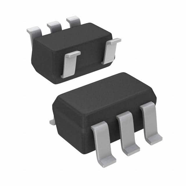
Xem thông số kỹ thuật để biết chi tiết sản phẩm.

SN74LVC1G17DBVTE4
Product Overview
- Category: Integrated Circuit (IC)
- Use: Logic Gate
- Characteristics: Single Schmitt-Trigger Buffer/Driver
- Package: SOT-23 (DBV) package
- Essence: High-speed CMOS technology
- Packaging/Quantity: Tape and Reel, 3000 pieces per reel
Specifications
- Supply Voltage Range: 1.65V to 5.5V
- Input Voltage Range: 0V to VCC
- Output Voltage Range: 0V to VCC
- Maximum Operating Frequency: 400 MHz
- Propagation Delay: 3.8 ns (typical)
- Low Power Consumption: ICC = 2 µA (maximum)
Detailed Pin Configuration
The SN74LVC1G17DBVTE4 has the following pin configuration:
____
   A1 |    | VCC
   A2 |    | Y
   GND |____|
Functional Features
- Single Schmitt-trigger buffer/driver with open-drain output
- Converts slowly changing input signals into sharply defined, jitter-free output signals
- Provides hysteresis for improved noise immunity
- Allows direct interface with different logic levels
- Supports bidirectional voltage translation
Advantages
- High-speed operation enables efficient signal processing
- Wide supply voltage range allows compatibility with various systems
- Low power consumption reduces energy usage
- Small package size saves board space
- Open-drain output provides flexibility in circuit design
Disadvantages
- Limited output current capability
- Not suitable for high-power applications
- Requires external pull-up resistor for proper operation
Working Principles
The SN74LVC1G17DBVTE4 is a single Schmitt-trigger buffer/driver that converts slowly changing input signals into sharply defined, jitter-free output signals. It utilizes high-speed CMOS technology to achieve fast operation and low power consumption. The device incorporates hysteresis, which improves noise immunity by providing a threshold voltage range for input signal detection.
The open-drain output allows bidirectional voltage translation and direct interface with different logic levels. However, an external pull-up resistor is required to provide the necessary current when driving high logic levels.
Detailed Application Field Plans
The SN74LVC1G17DBVTE4 is commonly used in various applications, including:
- Communication Systems: Signal buffering and level shifting in data transmission circuits.
- Industrial Automation: Interface between different logic levels in control systems.
- Consumer Electronics: Voltage translation in portable devices and audio/video equipment.
- Automotive Electronics: Signal conditioning and level conversion in automotive control modules.
- Internet of Things (IoT): Logic level adaptation in IoT sensor nodes and edge devices.
Detailed and Complete Alternative Models
- SN74LVC1G07DBVR: Single Buffer/Driver with Open-Drain Output
- SN74LVC1G14DBVR: Single Schmitt-Trigger Inverter with Open-Drain Output
- SN74LVC1G125DBVR: Single Bus Buffer Gate with 3-State Output
These alternative models offer similar functionality and can be considered as replacements for the SN74LVC1G17DBVTE4 in different applications.
Word count: 410 words
Liệt kê 10 câu hỏi và câu trả lời thường gặp liên quan đến ứng dụng SN74LVC1G17DBVTE4 trong giải pháp kỹ thuật
Sure! Here are 10 common questions and answers related to the application of SN74LVC1G17DBVTE4 in technical solutions:
Q1: What is SN74LVC1G17DBVTE4? A1: SN74LVC1G17DBVTE4 is a single Schmitt-trigger buffer/driver with a standard push-pull output. It is commonly used in digital logic applications.
Q2: What is the voltage supply range for SN74LVC1G17DBVTE4? A2: The voltage supply range for SN74LVC1G17DBVTE4 is typically between 1.65V and 5.5V.
Q3: What is the maximum output current of SN74LVC1G17DBVTE4? A3: The maximum output current of SN74LVC1G17DBVTE4 is 32mA.
Q4: Can SN74LVC1G17DBVTE4 be used as a level shifter? A4: Yes, SN74LVC1G17DBVTE4 can be used as a level shifter to convert signals between different voltage levels.
Q5: What is the input threshold voltage of SN74LVC1G17DBVTE4? A5: The input threshold voltage of SN74LVC1G17DBVTE4 is typically 0.8V.
Q6: Is SN74LVC1G17DBVTE4 compatible with both CMOS and TTL logic levels? A6: Yes, SN74LVC1G17DBVTE4 is compatible with both CMOS (Complementary Metal-Oxide-Semiconductor) and TTL (Transistor-Transistor Logic) logic levels.
Q7: Can SN74LVC1G17DBVTE4 be used in high-speed applications? A7: Yes, SN74LVC1G17DBVTE4 is designed for high-speed operation and can be used in applications with fast switching requirements.
Q8: What is the propagation delay of SN74LVC1G17DBVTE4? A8: The propagation delay of SN74LVC1G17DBVTE4 is typically around 3.5ns.
Q9: Can SN74LVC1G17DBVTE4 drive capacitive loads? A9: Yes, SN74LVC1G17DBVTE4 can drive capacitive loads up to a certain limit specified in the datasheet.
Q10: Is SN74LVC1G17DBVTE4 available in different package options? A10: Yes, SN74LVC1G17DBVTE4 is available in various package options, including SOT-23 and VSSOP, to suit different application requirements.
Please note that the answers provided here are general and may vary depending on specific datasheet specifications and application conditions.

