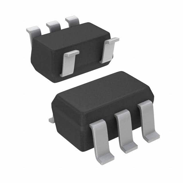
Xem thông số kỹ thuật để biết chi tiết sản phẩm.

SN74LVC1G14DBVTG4
Product Overview
- Category: Integrated Circuit
- Use: Logic Gate
- Characteristics: Single Schmitt-Trigger Inverter
- Package: SOT-23 (DBV)
- Essence: High-Speed CMOS Technology
- Packaging/Quantity: Tape and Reel, 3000 pieces per reel
Specifications
- Supply Voltage Range: 1.65V to 5.5V
- Input Voltage Range: -0.5V to VCC + 0.5V
- Output Voltage Range: 0V to VCC
- Maximum Operating Frequency: 100 MHz
- Propagation Delay: 3.8 ns (typical)
- Input Hysteresis: 0.5V (typical)
- Operating Temperature Range: -40°C to 85°C
Detailed Pin Configuration
The SN74LVC1G14DBVTG4 has a total of three pins:
- Pin 1: Input (IN) - Connects to the input signal.
- Pin 2: Ground (GND) - Connects to the ground reference.
- Pin 3: Output (OUT) - Provides the inverted output signal.
Functional Features
- Single Schmitt-Trigger Inverter: Converts input signals into inverted output signals with hysteresis for noise immunity.
- High-Speed CMOS Technology: Enables fast switching times and high-frequency operation.
- Wide Supply Voltage Range: Allows compatibility with various power supply levels.
- Low Power Consumption: Ideal for battery-powered applications.
- Small Package Size: SOT-23 package offers space-saving benefits.
Advantages
- Excellent Noise Immunity: The Schmitt-trigger input ensures reliable operation in noisy environments.
- Fast Switching Times: High-speed CMOS technology enables quick signal processing.
- Wide Supply Voltage Range: Provides flexibility in different voltage level applications.
- Low Power Consumption: Suitable for energy-efficient designs.
- Small Package Size: Saves board space and allows for compact designs.
Disadvantages
- Single Inverter: Limited functionality compared to more complex logic gates.
- Propagation Delay: Although relatively fast, it may not be suitable for ultra-high-speed applications.
Working Principles
The SN74LVC1G14DBVTG4 is a single Schmitt-trigger inverter. It utilizes CMOS technology to convert input signals into inverted output signals. The Schmitt-trigger input provides hysteresis, allowing the device to tolerate noise and provide reliable operation even in noisy environments. The high-speed CMOS technology ensures fast switching times and compatibility with various supply voltage levels.
Detailed Application Field Plans
The SN74LVC1G14DBVTG4 can be used in a wide range of applications, including:
- Signal Conditioning: The Schmitt-trigger input helps clean up noisy signals, making it suitable for signal conditioning applications.
- Oscillators: The inverter can be used as a building block for simple oscillators or clock generation circuits.
- Level Shifting: The device can be used to shift logic levels between different voltage domains.
- Sensor Interfaces: The Schmitt-trigger input can be used to interface with sensors that produce noisy signals.
Detailed and Complete Alternative Models
Some alternative models to the SN74LVC1G14DBVTG4 include:
- SN74LVC1G04DBVR: Single Inverter (NOT Gate)
- SN74LVC1G08DBVR: Single 2-Input AND Gate
- SN74LVC1G32DBVR: Single 2-Input OR Gate
- SN74LVC1G86DBVR: Single 2-Input XOR Gate
These alternatives provide different logic functions and can be used depending on the specific requirements of the application.
Word count: 413 words
Liệt kê 10 câu hỏi và câu trả lời thường gặp liên quan đến ứng dụng SN74LVC1G14DBVTG4 trong giải pháp kỹ thuật
Sure! Here are 10 common questions and answers related to the application of SN74LVC1G14DBVTG4 in technical solutions:
Q1: What is SN74LVC1G14DBVTG4? A1: SN74LVC1G14DBVTG4 is a single Schmitt-trigger inverter gate IC, commonly used in digital logic circuits.
Q2: What is the operating voltage range of SN74LVC1G14DBVTG4? A2: The operating voltage range of SN74LVC1G14DBVTG4 is from 1.65V to 5.5V.
Q3: What is the maximum output current of SN74LVC1G14DBVTG4? A3: The maximum output current of SN74LVC1G14DBVTG4 is typically 32mA.
Q4: Can SN74LVC1G14DBVTG4 be used as a level shifter? A4: Yes, SN74LVC1G14DBVTG4 can be used as a level shifter to convert signals between different voltage levels.
Q5: What is the propagation delay of SN74LVC1G14DBVTG4? A5: The propagation delay of SN74LVC1G14DBVTG4 is typically around 3.8ns.
Q6: Is SN74LVC1G14DBVTG4 suitable for high-speed applications? A6: Yes, SN74LVC1G14DBVTG4 is designed for high-speed operation and can be used in various high-frequency applications.
Q7: Can SN74LVC1G14DBVTG4 be used in battery-powered devices? A7: Yes, SN74LVC1G14DBVTG4 has a low power consumption and can be used in battery-powered devices.
Q8: What is the package type of SN74LVC1G14DBVTG4? A8: SN74LVC1G14DBVTG4 comes in a SOT-23-5 package.
Q9: Can SN74LVC1G14DBVTG4 be used in automotive applications? A9: Yes, SN74LVC1G14DBVTG4 is qualified for automotive applications and meets the necessary standards.
Q10: Are there any recommended application circuits available for SN74LVC1G14DBVTG4? A10: Yes, the datasheet of SN74LVC1G14DBVTG4 provides several recommended application circuits that can be used as reference designs.
Please note that these answers are general and may vary depending on specific use cases and requirements. It's always recommended to refer to the datasheet and consult with technical experts for accurate information.

