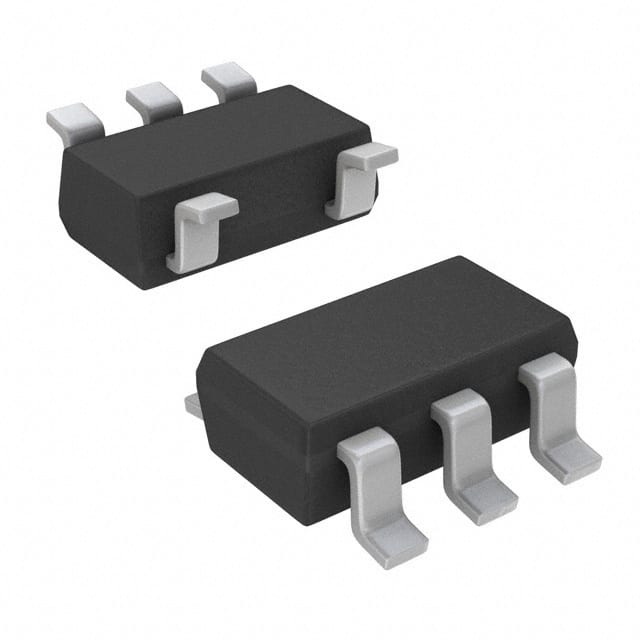
Xem thông số kỹ thuật để biết chi tiết sản phẩm.

SN74LVC1G00IDCKREP
Basic Information Overview
- Category: Integrated Circuit (IC)
- Use: Logic Gate
- Characteristics: Single 2-Input NAND Gate
- Package: SC-70 (6-Pin)
- Essence: High-Speed CMOS Technology
- Packaging/Quantity: Tape and Reel, 3000 pieces per reel
Specifications
- Supply Voltage Range: 1.65V to 5.5V
- Input Voltage Range: 0V to VCC
- Output Voltage Range: 0V to VCC
- Maximum Operating Frequency: 400 MHz
- Propagation Delay: 3.8 ns (typical)
- Low Power Consumption: ICC = 1 µA (maximum)
Detailed Pin Configuration
The SN74LVC1G00IDCKREP has the following pin configuration:
____
   A --|    |-- VCC
   B --|    |-- Y
 GND --|____|-- NC
Functional Features
- Single 2-Input NAND gate with Schmitt-trigger inputs
- Compatible with TTL input levels
- Provides standard CMOS output levels
- Supports mixed-mode voltage operation
- Allows direct interface with 3.3V and 5V systems
- High-speed operation for improved system performance
- Low power consumption for energy-efficient designs
Advantages and Disadvantages
Advantages: - Compact package size enables space-saving designs - Wide supply voltage range allows compatibility with various systems - High-speed operation enhances overall system performance - Low power consumption reduces energy consumption
Disadvantages: - Limited to a single 2-input NAND gate functionality - Not suitable for applications requiring more complex logic functions
Working Principles
The SN74LVC1G00IDCKREP is based on high-speed CMOS technology. It operates as a 2-input NAND gate, where the output is low only when both inputs are high. The Schmitt-trigger inputs ensure reliable operation even in the presence of noisy or slow input signals. The IC can be powered by a supply voltage ranging from 1.65V to 5.5V, making it compatible with a wide range of systems.
Detailed Application Field Plans
The SN74LVC1G00IDCKREP finds applications in various fields, including: 1. Consumer Electronics: Used in portable devices, such as smartphones and tablets, for logic operations. 2. Industrial Automation: Employed in control systems and PLCs for signal processing and logic functions. 3. Automotive Electronics: Integrated into automotive modules for reliable and efficient logic operations. 4. Communication Systems: Utilized in networking equipment and data communication devices for signal processing.
Detailed and Complete Alternative Models
Some alternative models that offer similar functionality to the SN74LVC1G00IDCKREP include: - SN74LVC1G00DBVR - SN74LVC1G00DCKR - SN74LVC1G00DRLR - SN74LVC1G00YZPR
These alternatives provide the same 2-input NAND gate functionality and are also based on high-speed CMOS technology. However, they may differ in package type, pin configuration, or other minor specifications.
Word count: 346 words
Liệt kê 10 câu hỏi và câu trả lời thường gặp liên quan đến ứng dụng SN74LVC1G00IDCKREP trong giải pháp kỹ thuật
Sure! Here are 10 common questions and answers related to the application of SN74LVC1G00IDCKREP:
Q1: What is SN74LVC1G00IDCKREP? A1: SN74LVC1G00IDCKREP is a single 2-input NAND gate IC (integrated circuit) that belongs to the LVC (Low-Voltage CMOS) family. It is commonly used in digital logic circuits.
Q2: What is the operating voltage range of SN74LVC1G00IDCKREP? A2: The operating voltage range of SN74LVC1G00IDCKREP is from 1.65V to 5.5V.
Q3: What is the maximum output current of SN74LVC1G00IDCKREP? A3: The maximum output current of SN74LVC1G00IDCKREP is typically 32mA.
Q4: Can SN74LVC1G00IDCKREP be used for level shifting between different voltage domains? A4: Yes, SN74LVC1G00IDCKREP can be used for level shifting as it supports multiple voltage levels within its operating range.
Q5: What is the typical propagation delay of SN74LVC1G00IDCKREP? A5: The typical propagation delay of SN74LVC1G00IDCKREP is around 4.3ns.
Q6: Is SN74LVC1G00IDCKREP suitable for high-speed applications? A6: Yes, SN74LVC1G00IDCKREP is suitable for high-speed applications due to its low propagation delay and fast switching characteristics.
Q7: Can SN74LVC1G00IDCKREP drive capacitive loads? A7: Yes, SN74LVC1G00IDCKREP can drive capacitive loads up to a certain limit. However, it is recommended to use additional buffering if the load capacitance exceeds the specified value.
Q8: What is the package type of SN74LVC1G00IDCKREP? A8: SN74LVC1G00IDCKREP is available in a small SOT-353 package.
Q9: Can SN74LVC1G00IDCKREP be used in battery-powered applications? A9: Yes, SN74LVC1G00IDCKREP is suitable for battery-powered applications as it operates at low voltages and has low power consumption.
Q10: Is SN74LVC1G00IDCKREP RoHS compliant? A10: Yes, SN74LVC1G00IDCKREP is RoHS (Restriction of Hazardous Substances) compliant, ensuring it meets environmental regulations.
Please note that these answers are general and may vary depending on specific datasheet specifications and application requirements.

