

Xem thông số kỹ thuật để biết chi tiết sản phẩm.
SN74LV4T125RGYR
Product Overview
- Category: Integrated Circuit (IC)
- Use: Logic Level Shifter
- Characteristics: Low-voltage, Quad-Bus Buffer Gate with 3-State Outputs
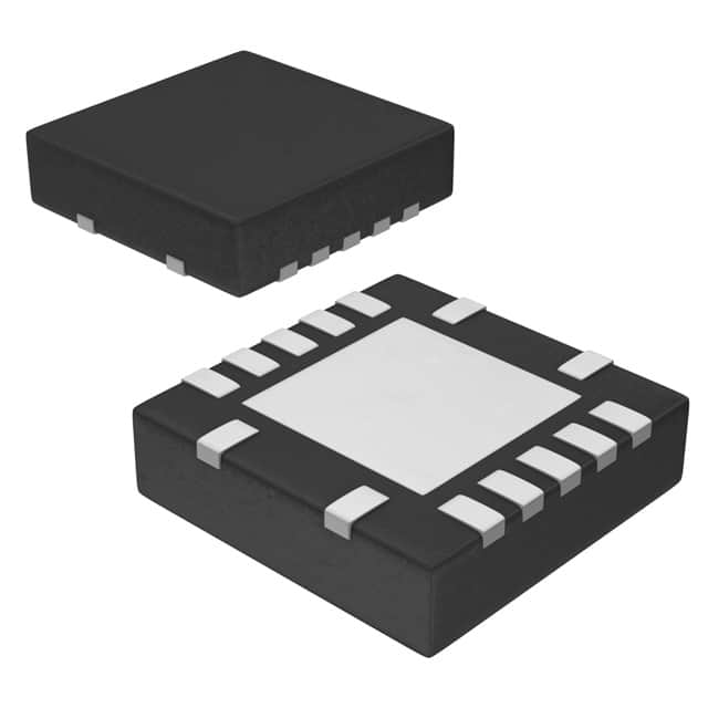
- Package: VQFN-14
- Essence: This IC is designed to shift logic levels between different voltage domains, allowing for seamless communication between devices operating at different voltage levels.
- Packaging/Quantity: Available in reels of 2500 units.
Specifications
- Supply Voltage Range: 1.65V to 5.5V
- High-Level Input Voltage: 2.3V to VCC + 0.5V
- Low-Level Input Voltage: -0.5V to 0.8V
- High-Level Output Voltage: VCC - 0.5V
- Low-Level Output Voltage: 0.5V
- Maximum Operating Frequency: 100 MHz
- Number of Channels: 4
- Output Drive Capability: ±24 mA
- Operating Temperature Range: -40°C to +85°C
Detailed Pin Configuration
The SN74LV4T125RGYR has a VQFN-14 package with the following pin configuration:
___________
      |           |
   1  |         14 |  VCC
   2  |         13 |  A1
   3  |         12 |  OE#
   4  |         11 |  Y1
   5  |         10 |  GND
   6  |          9 |  Y2
   7  |          8 |  A2
      |___________|
Functional Features
- Quad-bus buffer gate with 3-state outputs.
- Allows bidirectional level shifting between different voltage domains.
- Supports voltage translation between 1.65V and 5.5V.
- Provides high-speed logic level shifting with minimal propagation delay.
- Enables seamless communication between devices operating at different voltage levels.
Advantages and Disadvantages
Advantages: - Wide supply voltage range allows compatibility with various systems. - High output drive capability enables driving capacitive loads. - Low propagation delay ensures fast signal transmission. - 3-state outputs provide flexibility in controlling bus lines.
Disadvantages: - Limited to 4 channels, may not be suitable for applications requiring more channels. - Operating frequency limited to 100 MHz, may not be suitable for high-speed applications.
Working Principles
The SN74LV4T125RGYR operates by receiving input signals from one voltage domain and translating them to the desired voltage level of another domain. It utilizes a combination of MOSFETs and control circuitry to achieve bidirectional level shifting. The OE# pin controls the output enable/disable function, allowing the device to enter a high-impedance state when disabled.
Detailed Application Field Plans
The SN74LV4T125RGYR is commonly used in various applications where logic level shifting is required. Some typical application fields include:
- Microcontroller interfacing: Allows communication between microcontrollers operating at different voltage levels.
- Sensor networks: Facilitates data exchange between sensors operating at different voltage domains.
- Industrial automation: Enables integration of devices with varying voltage requirements in industrial control systems.
- IoT devices: Supports connectivity between IoT devices with different voltage levels.
- Battery-powered systems: Allows efficient power management by enabling communication between low-voltage battery-powered devices and higher voltage components.
Detailed and Complete Alternative Models
- SN74LVC4T125: Similar to SN74LV4T125RGYR but operates at a wider supply voltage range of 1.65V to 5.5V.
- SN74LVC4T125DBVR: SMD package variant with the same functionality and characteristics as SN74LV4T125RGYR.
- SN74LVC4T125PW: TSSOP package variant suitable for surface mount applications.
These alternative models provide similar logic level shifting capabilities and can be considered based on specific application requirements.
Word count: 480 words
Liệt kê 10 câu hỏi và câu trả lời thường gặp liên quan đến ứng dụng SN74LV4T125RGYR trong giải pháp kỹ thuật
Sure! Here are 10 common questions and answers related to the application of SN74LV4T125RGYR:
Question: What is SN74LV4T125RGYR?
- Answer: SN74LV4T125RGYR is a quad bus buffer gate with 3-state outputs, designed for voltage translation.Question: What is the operating voltage range of SN74LV4T125RGYR?
- Answer: The operating voltage range is from 1.65V to 5.5V.Question: What is the maximum output current of SN74LV4T125RGYR?
- Answer: The maximum output current is ±12mA.Question: Can SN74LV4T125RGYR be used for level shifting between different voltage domains?
- Answer: Yes, SN74LV4T125RGYR can be used for level shifting between different voltage domains.Question: How many channels does SN74LV4T125RGYR have?
- Answer: SN74LV4T125RGYR has four channels.Question: What is the propagation delay of SN74LV4T125RGYR?
- Answer: The propagation delay is typically 4.7ns.Question: Is SN74LV4T125RGYR suitable for high-speed applications?
- Answer: Yes, SN74LV4T125RGYR is suitable for high-speed applications due to its low propagation delay.Question: Can SN74LV4T125RGYR handle bidirectional data flow?
- Answer: No, SN74LV4T125RGYR is unidirectional and can only handle data flow in one direction.Question: What is the package type of SN74LV4T125RGYR?
- Answer: SN74LV4T125RGYR comes in a small 14-pin VQFN package.Question: Are there any special considerations when using SN74LV4T125RGYR?
- Answer: It is important to ensure that the voltage levels and power supply requirements are within the specified range for proper operation.
Please note that these answers are general and may vary depending on the specific application and requirements.