Xem thông số kỹ thuật để biết chi tiết sản phẩm.

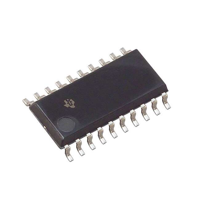
SN74LS593NSR
Product Overview
- Category: Integrated Circuit
- Use: Shift Register
- Characteristics: TTL Logic, 8-bit parallel-in/serial-out shift register
- Package: SOIC (Small Outline Integrated Circuit)
- Essence: Serial data is loaded into the register through parallel inputs and shifted out serially
- Packaging/Quantity: Tape and Reel, 2500 units per reel
Specifications
- Supply Voltage: 4.75V to 5.25V
- Operating Temperature Range: -40°C to +85°C
- Input Voltage High Level: 2.0V min
- Input Voltage Low Level: 0.8V max
- Output Voltage High Level: 2.7V min
- Output Voltage Low Level: 0.5V max
- Maximum Clock Frequency: 30 MHz
Pin Configuration
The SN74LS593NSR has a total of 16 pins. The pin configuration is as follows:
- QA (Output A)
- QB (Output B)
- QC (Output C)
- QD (Output D)
- QE (Output E)
- QF (Output F)
- QG (Output G)
- QH (Output H)
- SER (Serial Data Input)
- RCLK (Register Clock Input)
- SRCLK (Shift Register Clock Input)
- OE (Output Enable)
- MR (Master Reset)
- VCC (Supply Voltage)
- GND (Ground)
- QA' (Complement of Output A)
Functional Features
- Parallel-in/serial-out operation
- Synchronous shifting of data
- Output enable control for tri-state outputs
- Master reset for clearing the register
- Complementary output available
Advantages and Disadvantages
Advantages: - High-speed operation - Easy integration into digital systems - Compact package size
Disadvantages: - Limited number of outputs (8 bits) - Requires external clock signals for proper operation
Working Principles
The SN74LS593NSR is a TTL logic device that functions as an 8-bit parallel-in/serial-out shift register. It allows data to be loaded into the register through parallel inputs and then shifted out serially. The shifting of data is controlled by clock signals applied to the SRCLK input. The RCLK input is used to latch the parallel data into the register. The OE input enables or disables the outputs, allowing for tri-state operation.
Detailed Application Field Plans
The SN74LS593NSR can be used in various applications, including:
- Serial data communication systems
- Data storage and retrieval systems
- Digital signal processing
- Microcontroller interfacing
- Industrial automation
Alternative Models
Other alternative models that can be used as replacements for the SN74LS593NSR include:
- CD74HC595E
- SN74HC595N
- MC74HC595AD
These models offer similar functionality and can be used interchangeably depending on specific requirements.
In conclusion, the SN74LS593NSR is a versatile integrated circuit that serves as an 8-bit parallel-in/serial-out shift register. Its compact package, high-speed operation, and easy integration make it suitable for various digital applications. However, its limited number of outputs and reliance on external clock signals should be considered when selecting this device for a particular project.
Liệt kê 10 câu hỏi và câu trả lời thường gặp liên quan đến ứng dụng SN74LS593NSR trong giải pháp kỹ thuật
Sure! Here are 10 common questions and answers related to the application of SN74LS593NSR:
Question: What is SN74LS593NSR?
Answer: SN74LS593NSR is a 8-bit shift register with output latches, commonly used in digital circuits.Question: What is the maximum clock frequency for SN74LS593NSR?
Answer: The maximum clock frequency for SN74LS593NSR is typically around 25 MHz.Question: How many bits can SN74LS593NSR store?
Answer: SN74LS593NSR can store up to 8 bits of data.Question: Can SN74LS593NSR be cascaded to increase the number of bits?
Answer: Yes, SN74LS593NSR can be cascaded to increase the number of bits by connecting the output of one shift register to the input of another.Question: What is the purpose of the output latches in SN74LS593NSR?
Answer: The output latches in SN74LS593NSR hold the data at the outputs until new data is shifted in, allowing for stable output values.Question: What is the power supply voltage range for SN74LS593NSR?
Answer: The power supply voltage range for SN74LS593NSR is typically between 4.75V and 5.25V.Question: Can SN74LS593NSR be used in both parallel and serial data transfer applications?
Answer: Yes, SN74LS593NSR can be used in both parallel and serial data transfer applications depending on how it is configured.Question: What is the typical propagation delay of SN74LS593NSR?
Answer: The typical propagation delay of SN74LS593NSR is around 15 ns.Question: Can SN74LS593NSR be used in both synchronous and asynchronous clocking systems?
Answer: Yes, SN74LS593NSR can be used in both synchronous and asynchronous clocking systems depending on the application requirements.Question: What are some common applications of SN74LS593NSR?
Answer: Some common applications of SN74LS593NSR include data storage, data transfer, serial-to-parallel conversion, and parallel-to-serial conversion in digital systems.

