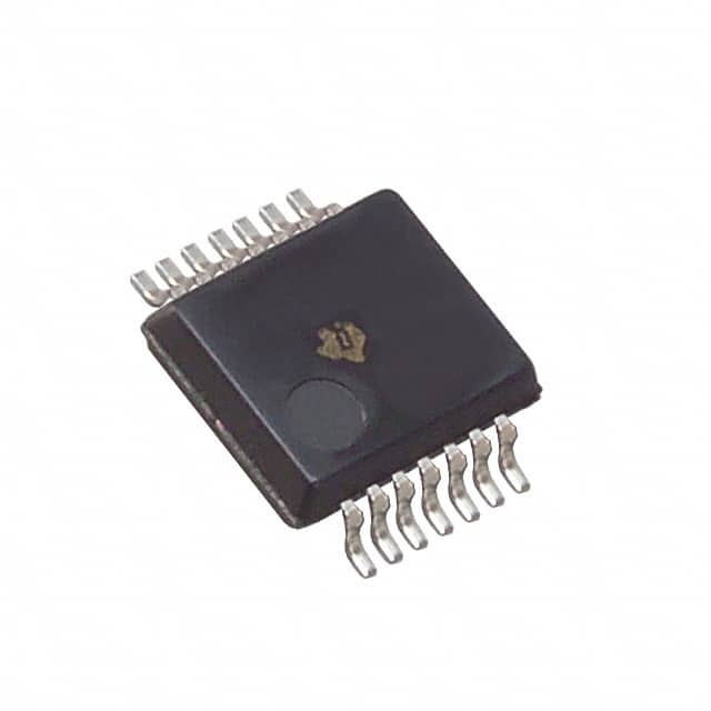
Xem thông số kỹ thuật để biết chi tiết sản phẩm.

SN74HC20DBRG4
Product Overview
- Category: Integrated Circuit (IC)
- Use: Logic Gate
- Characteristics: Dual 4-input NAND gate
- Package: SOIC-14
- Essence: High-speed CMOS technology
- Packaging/Quantity: Tape and Reel, 2500 pieces per reel
Specifications
- Supply Voltage Range: 2V to 6V
- Input Voltage Range: 0V to VCC
- Output Voltage Range: 0V to VCC
- Operating Temperature Range: -40°C to +85°C
- Propagation Delay Time: 9 ns (typical)
- Maximum Quiescent Current: 1 µA at 5.5V
- Maximum Input Current: ±1 µA at 5.5V
- Maximum Output Current: ±8 mA at 5.5V
Detailed Pin Configuration
The SN74HC20DBRG4 has a total of 14 pins arranged as follows:
__    __
   A1 | 1  14 | VCC
   B1 | 2  13 | C1
   A2 | 3  12 | D1
   B2 | 4  11 | C2
   Y1 | 5  10 | D2
  GND | 6   9 | Y2
   A3 | 7   8 | B3
       --------
Functional Features
- Dual 4-input NAND gate with independent inputs
- High-speed operation due to CMOS technology
- Schmitt-trigger input allows for noisy signal processing
- Wide supply voltage range enables compatibility with various systems
- Low power consumption in both active and standby modes
Advantages and Disadvantages
Advantages
- Fast propagation delay time ensures quick response in logic operations
- Schmitt-trigger input enhances noise immunity and signal integrity
- Wide supply voltage range allows for versatile applications
- Low power consumption makes it suitable for battery-powered devices
Disadvantages
- Limited number of inputs (4 per gate)
- Not suitable for high-voltage applications (>6V)
Working Principles
The SN74HC20DBRG4 is based on high-speed CMOS technology, which combines the advantages of both CMOS and TTL logic families. It operates as a dual 4-input NAND gate, where each gate has independent inputs. The Schmitt-trigger input provides hysteresis, allowing the device to tolerate noisy input signals without false triggering. The output is determined by the logical AND operation of all four inputs.
Detailed Application Field Plans
The SN74HC20DBRG4 can be used in various digital logic applications, including:
- Data processing systems
- Arithmetic circuits
- Memory address decoding
- Clock synchronization circuits
- Control systems
- Signal conditioning circuits
- Industrial automation
Detailed and Complete Alternative Models
- CD4012BE: Dual 4-input NAND gate, DIP-14 package
- MC14093BCP: Quad 2-input NAND gate, PDIP-14 package
- 74LS20: Dual 4-input NAND gate, DIP-14 package
- CD4073B: Triple 3-input AND gate, SOIC-14 package
- SN74HC21D: Dual 4-input AND gate, SOIC-14 package
These alternative models offer similar functionality and can be used as substitutes for the SN74HC20DBRG4 depending on specific requirements.
In conclusion, the SN74HC20DBRG4 is a dual 4-input NAND gate IC that offers high-speed operation, noise immunity, and low power consumption. It finds applications in various digital logic systems and can be replaced by alternative models with similar functionality.
Liệt kê 10 câu hỏi và câu trả lời thường gặp liên quan đến ứng dụng SN74HC20DBRG4 trong giải pháp kỹ thuật
Sure! Here are 10 common questions and answers related to the application of SN74HC20DBRG4 in technical solutions:
Q: What is SN74HC20DBRG4? A: SN74HC20DBRG4 is a dual 4-input NAND gate integrated circuit (IC) that can be used in various digital logic applications.
Q: What is the operating voltage range for SN74HC20DBRG4? A: The operating voltage range for SN74HC20DBRG4 is typically between 2V and 6V.
Q: What is the maximum output current of SN74HC20DBRG4? A: The maximum output current of SN74HC20DBRG4 is approximately 5.2mA.
Q: Can SN74HC20DBRG4 be used in high-speed applications? A: Yes, SN74HC20DBRG4 is designed for high-speed operation and can be used in applications with fast switching requirements.
Q: How many inputs does SN74HC20DBRG4 have? A: SN74HC20DBRG4 has two independent 4-input NAND gates, totaling eight inputs.
Q: What is the propagation delay of SN74HC20DBRG4? A: The typical propagation delay of SN74HC20DBRG4 is around 9ns.
Q: Can SN74HC20DBRG4 be used in both CMOS and TTL logic systems? A: Yes, SN74HC20DBRG4 is compatible with both CMOS and TTL logic levels, making it versatile for different system designs.
Q: Is SN74HC20DBRG4 available in different package options? A: Yes, SN74HC20DBRG4 is available in various package options, including SOIC, TSSOP, and VQFN.
Q: What is the power dissipation of SN74HC20DBRG4? A: The power dissipation of SN74HC20DBRG4 is typically around 25mW.
Q: Can SN74HC20DBRG4 be used in automotive applications? A: Yes, SN74HC20DBRG4 is qualified for automotive applications and can operate within the specified temperature range for automotive environments.
Please note that these answers are general and may vary depending on specific datasheet specifications and application requirements.

