

Xem thông số kỹ thuật để biết chi tiết sản phẩm.
SN74AUP3G06DQER
Product Overview
- Category: Integrated Circuit (IC)
- Use: Logic Gate
- Characteristics: High-speed, low-power, voltage-level translation
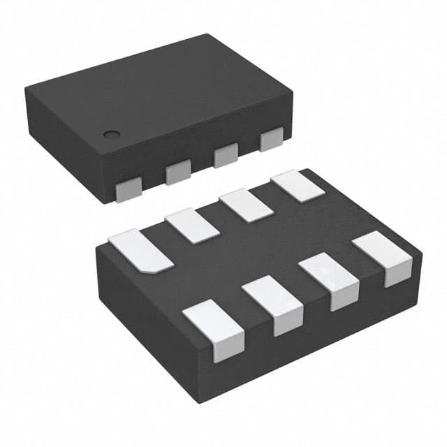
- Package: VSSOP (Very Small Outline Package)
- Essence: Inverter Buffer
- Packaging/Quantity: Tape and Reel, 3000 pieces per reel
Specifications
- Supply Voltage Range: 0.8V to 3.6V
- Input Voltage Range: 0V to VCC
- Output Voltage Range: 0V to VCC
- Maximum Operating Frequency: 500 MHz
- Propagation Delay: 1.9 ns (typical)
- Input Capacitance: 2 pF (typical)
- Output Capacitance: 2 pF (typical)
Detailed Pin Configuration
The SN74AUP3G06DQER has a total of six pins:
- GND: Ground pin
- A: Input pin for logic signal
- Y: Output pin for inverted logic signal
- VCC: Positive power supply pin
- B: Input pin for logic signal
- YB: Output pin for inverted logic signal
Functional Features
- Inverts the logic level of input signals
- Provides voltage-level translation between different logic families
- High-speed operation with low power consumption
- Supports wide supply voltage range for compatibility
Advantages
- Compact VSSOP package allows for space-saving designs
- Wide supply voltage range enables versatile applications
- High-speed operation enhances overall system performance
- Low power consumption contributes to energy efficiency
Disadvantages
- Limited number of inputs and outputs
- Not suitable for high-current applications
- May require additional components for specific circuit configurations
Working Principles
The SN74AUP3G06DQER is an inverter buffer that operates by converting the input logic level to its complemented output logic level. It utilizes a combination of transistors and resistors to achieve this inversion. The device also performs voltage-level translation, allowing compatibility between different logic families by adapting the signal levels accordingly.
Detailed Application Field Plans
The SN74AUP3G06DQER finds applications in various fields, including:
- Consumer Electronics: Used in smartphones, tablets, and portable devices for logic level conversion and signal inversion.
- Automotive: Employed in automotive electronics for voltage-level translation and logic signal processing.
- Industrial Automation: Integrated into control systems and PLCs (Programmable Logic Controllers) for logic signal conditioning and interfacing.
- Communication Systems: Utilized in networking equipment and data communication devices for signal conversion and level shifting.
Detailed and Complete Alternative Models
- SN74LVC1G06DBVR: Inverter Buffer with Schmitt Trigger Input
- SN74LV1T34DBVR: Single Buffer Gate with 3-State Output
- SN74AHC1G04DBVR: Inverter Gate with Open-Drain Output
- SN74HCT04DBVR: Hex Inverter Gate
These alternative models offer similar functionality and can be used as substitutes for the SN74AUP3G06DQER in various applications.
Word count: 389 words
Liệt kê 10 câu hỏi và câu trả lời thường gặp liên quan đến ứng dụng SN74AUP3G06DQER trong giải pháp kỹ thuật
Sure! Here are 10 common questions and answers related to the application of SN74AUP3G06DQER in technical solutions:
Q: What is SN74AUP3G06DQER? A: SN74AUP3G06DQER is a triple inverter gate IC (Integrated Circuit) that can be used for signal inversion and level shifting.
Q: What is the voltage range supported by SN74AUP3G06DQER? A: SN74AUP3G06DQER supports a voltage range from 0.8V to 3.6V.
Q: Can SN74AUP3G06DQER be used for level shifting between different voltage domains? A: Yes, SN74AUP3G06DQER can be used for level shifting between different voltage domains as long as they fall within the supported voltage range.
Q: What is the maximum output current of SN74AUP3G06DQER? A: The maximum output current of SN74AUP3G06DQER is typically around 32mA.
Q: Can SN74AUP3G06DQER be used for bidirectional level shifting? A: No, SN74AUP3G06DQER is not designed for bidirectional level shifting. It can only shift signals from one voltage domain to another.
Q: Is SN74AUP3G06DQER suitable for high-speed applications? A: Yes, SN74AUP3G06DQER is designed for high-speed applications and has a propagation delay of typically 2.7ns.
Q: Can SN74AUP3G06DQER be used in battery-powered applications? A: Yes, SN74AUP3G06DQER is suitable for battery-powered applications as it operates within a low voltage range and has low power consumption.
Q: What is the package type of SN74AUP3G06DQER? A: SN74AUP3G06DQER comes in a small SOT-23-6 package.
Q: Can SN74AUP3G06DQER be used in automotive applications? A: Yes, SN74AUP3G06DQER is AEC-Q100 qualified, making it suitable for automotive applications.
Q: Are there any recommended operating conditions for SN74AUP3G06DQER? A: Yes, some recommended operating conditions include a supply voltage between 0.8V and 3.6V, an ambient temperature range of -40°C to 85°C, and a maximum input voltage of VCC + 0.5V.
Please note that these answers are general and may vary depending on the specific requirements and datasheet of SN74AUP3G06DQER.