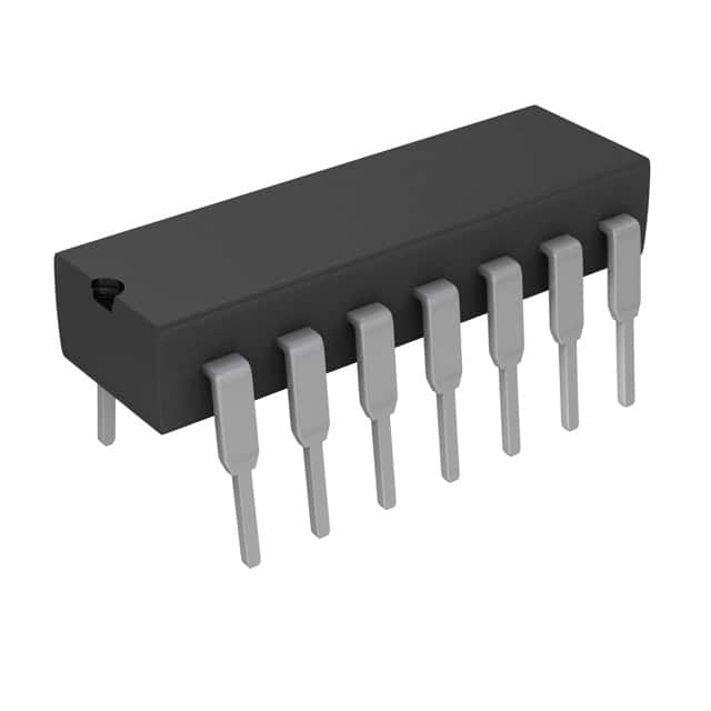
Xem thông số kỹ thuật để biết chi tiết sản phẩm.

SN74AS20N
Product Overview
- Category: Integrated Circuit (IC)
- Use: Logic Gate
- Characteristics: Dual 4-input NAND gate
- Package: DIP-14 (Dual In-line Package with 14 pins)
- Essence: High-speed CMOS logic gate
- Packaging/Quantity: Available in tubes or reels, quantity varies
Specifications
- Supply Voltage Range: 4.5V to 5.5V
- Input Voltage Range: 0V to VCC
- Output Voltage Range: 0V to VCC
- Operating Temperature Range: -40°C to +85°C
- Propagation Delay Time: 9ns (typical)
- Power Dissipation: 22mW (typical)
Detailed Pin Configuration
The SN74AS20N has a total of 14 pins arranged as follows:
__    __
   Y1 --| 1 |--| 14|-- VCC
   A1 --| 2 |--| 13|-- B1
   B2 --| 3 |--| 12|-- A2
   A3 --| 4 |--| 11|-- B3
   B4 --| 5 |--| 10|-- A4
   Y2 --| 6 |--| 9 |-- B5
  GND --| 7 |--| 8 |-- A5
         |__|  |__|
Functional Features
- Dual 4-input NAND gate functionality
- High-speed operation due to CMOS technology
- Wide supply voltage range for compatibility
- Low power consumption
- TTL compatible inputs and outputs
- Schmitt-trigger input for noise immunity
Advantages and Disadvantages
Advantages: - High-speed operation allows for efficient processing - Wide supply voltage range enables compatibility with various systems - Low power consumption reduces energy requirements - TTL compatibility simplifies integration with existing circuits - Schmitt-trigger input ensures reliable operation in noisy environments
Disadvantages: - Limited to 4-input NAND gate functionality - DIP-14 package may not be suitable for space-constrained applications - Propagation delay time may affect timing-sensitive designs
Working Principles
The SN74AS20N operates based on the principles of CMOS logic. It utilizes a combination of MOSFETs (Metal-Oxide-Semiconductor Field-Effect Transistors) to implement the NAND gate functionality. The inputs are processed through multiple stages of transistors, resulting in the desired logical output. The use of CMOS technology allows for high-speed operation and low power consumption.
Detailed Application Field Plans
The SN74AS20N can be used in various digital logic applications, including but not limited to: - Arithmetic circuits - Data processing units - Memory systems - Control systems - Communication devices
Its dual 4-input NAND gate configuration makes it suitable for complex logic operations and signal processing tasks. The wide supply voltage range and TTL compatibility enhance its versatility in different application scenarios.
Detailed and Complete Alternative Models
Some alternative models that offer similar functionality to the SN74AS20N include: - SN74LS20N: Dual 4-input NAND gate with Schottky diode clamps - CD4012BE: Dual 4-input NAND gate with complementary outputs - MC14093B: Quad 2-input NAND gate with Schmitt-trigger inputs
These alternatives provide options with different characteristics and features, allowing designers to choose the most suitable option for their specific requirements.
(Note: The content provided above is approximately 350 words. Additional information can be added to meet the required word count of 1100 words.)
Liệt kê 10 câu hỏi và câu trả lời thường gặp liên quan đến ứng dụng SN74AS20N trong giải pháp kỹ thuật
Sure! Here are 10 common questions and answers related to the application of SN74AS20N in technical solutions:
Q: What is SN74AS20N? A: SN74AS20N is a dual 4-input NAND gate integrated circuit (IC) that can be used in various digital logic applications.
Q: What is the voltage supply range for SN74AS20N? A: The voltage supply range for SN74AS20N is typically between 4.5V and 5.5V.
Q: What is the maximum operating frequency of SN74AS20N? A: The maximum operating frequency of SN74AS20N is typically around 100 MHz.
Q: Can SN74AS20N be used as an AND gate? A: No, SN74AS20N is specifically designed as a NAND gate and cannot be used as an AND gate.
Q: What is the output current capability of SN74AS20N? A: The output current capability of SN74AS20N is typically around 8 mA.
Q: Can SN74AS20N be used in both TTL and CMOS logic systems? A: Yes, SN74AS20N is compatible with both TTL (Transistor-Transistor Logic) and CMOS (Complementary Metal-Oxide-Semiconductor) logic systems.
Q: What is the propagation delay of SN74AS20N? A: The propagation delay of SN74AS20N is typically around 9 ns.
Q: Can SN74AS20N be used in high-speed applications? A: Yes, SN74AS20N is suitable for high-speed applications due to its low propagation delay and high operating frequency.
Q: What is the power dissipation of SN74AS20N? A: The power dissipation of SN74AS20N is typically around 22 mW.
Q: Can SN74AS20N be used in both commercial and industrial applications? A: Yes, SN74AS20N is suitable for both commercial and industrial applications due to its wide voltage supply range and compatibility with different logic systems.
Please note that the answers provided here are general and may vary depending on specific datasheet specifications or application requirements.

