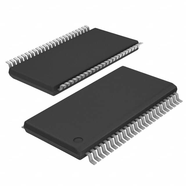
Xem thông số kỹ thuật để biết chi tiết sản phẩm.

SN74ALVCH16973DGVR
Basic Information Overview
- Category: Integrated Circuit (IC)
- Use: Digital Logic Device
- Characteristics:
- Low-voltage CMOS technology
- High-speed operation
- Wide operating voltage range
- Multiple I/O compatibility
- Package: VSSOP (Very Small Outline Package)
- Essence: Flip-Flop Register
- Packaging/Quantity: Tape and Reel, 2500 units per reel
Specifications
- Logic Family: ALVCH
- Number of Bits: 16
- Number of Registers: 2
- Supply Voltage Range: 1.65V to 3.6V
- Input/Output Compatibility: TTL, LVTTL, LVCMOS
- Operating Temperature Range: -40°C to +85°C
- Output Drive Strength: ±24mA
- Propagation Delay: 2.5ns (typical)
Detailed Pin Configuration
The SN74ALVCH16973DGVR has a total of 56 pins. The pin configuration is as follows:
- GND
- D1A
- D1B
- D1C
- D1D
- D1E
- D1F
- D1G
- D1H
- Q1A
- Q1B
- Q1C
- Q1D
- Q1E
- Q1F
- Q1G
- Q1H
- OE1
- CLK1
- CP1
- MR1
- PR1
- VCC
- Q2A
- Q2B
- Q2C
- Q2D
- Q2E
- Q2F
- Q2G
- Q2H
- OE2
- CLK2
- CP2
- MR2
- PR2
- D2A
- D2B
- D2C
- D2D
- D2E
- D2F
- D2G
- D2H
- GND
- D1J
- D1K
- D1L
- D1M
- D1N
- D1P
- D1R
- D1S
- VCC
- D2J
- D2K
Functional Features
- Flip-Flop Register: The SN74ALVCH16973DGVR consists of two 8-bit flip-flop registers that can store and transfer data.
- High-Speed Operation: The IC operates at high speeds, making it suitable for applications requiring fast data processing.
- Wide Operating Voltage Range: It can operate within a voltage range of 1.65V to 3.6V, providing flexibility in various systems.
- Multiple I/O Compatibility: The device is compatible with TTL, LVTTL, and LVCMOS logic levels, allowing easy integration into different digital systems.
Advantages and Disadvantages
Advantages: - Low-voltage CMOS technology ensures low power consumption. - High-speed operation enables efficient data processing. - Wide operating voltage range provides versatility in system design. - Multiple I/O compatibility simplifies integration into various digital systems.
Disadvantages: - Limited number of registers (2) may not be sufficient for complex applications requiring more storage capacity. - Propagation delay of 2.5ns (typical) may not meet the requirements of ultra-high-speed applications.
Working Principles
The SN74ALVCH16973DGVR operates based on the principles of flip-flop registers. It stores and transfers data using two 8-bit registers. The input data is latched into the registers based on clock signals, and the stored data can be accessed through the output pins. The device operates at high speeds and is compatible with various logic levels, making it suitable for a wide range of digital applications.
Detailed Application Field Plans
The SN74ALVCH16973DGVR can be used in various applications, including: 1. Data Storage Systems: The flip-flop registers can store data temporarily, making the IC suitable for use in memory systems. 2. Communication Devices: The high-speed operation and multiple I/O compatibility make it ideal for use in communication devices such as routers, switches, and modems. 3. Industrial Control Systems: The wide operating voltage range and low power consumption make it suitable for use in industrial control systems that require reliable and efficient data processing. 4. Automotive Electronics: The IC's ability to operate within a wide temperature range (-40°C to +
Liệt kê 10 câu hỏi và câu trả lời thường gặp liên quan đến ứng dụng SN74ALVCH16973DGVR trong giải pháp kỹ thuật
Sure! Here are 10 common questions and answers related to the application of SN74ALVCH16973DGVR:
Q: What is the SN74ALVCH16973DGVR? A: The SN74ALVCH16973DGVR is a 16-bit transparent D-type latch with 3-state outputs, designed for low-voltage (1.65V to 3.6V) applications.
Q: What is the maximum operating frequency of the SN74ALVCH16973DGVR? A: The maximum operating frequency of the SN74ALVCH16973DGVR is typically around 500 MHz.
Q: Can I use the SN74ALVCH16973DGVR in a 5V system? A: No, the SN74ALVCH16973DGVR is not recommended for use in 5V systems as it operates at lower voltage levels.
Q: How many output pins does the SN74ALVCH16973DGVR have? A: The SN74ALVCH16973DGVR has 16 output pins, one for each bit of the latch.
Q: What is the power supply voltage range for the SN74ALVCH16973DGVR? A: The power supply voltage range for the SN74ALVCH16973DGVR is from 1.65V to 3.6V.
Q: Can I connect the outputs of multiple SN74ALVCH16973DGVR devices together? A: Yes, the outputs of multiple SN74ALVCH16973DGVR devices can be connected together to form larger data buses.
Q: Does the SN74ALVCH16973DGVR have internal pull-up or pull-down resistors? A: No, the SN74ALVCH16973DGVR does not have internal pull-up or pull-down resistors.
Q: What is the typical propagation delay of the SN74ALVCH16973DGVR? A: The typical propagation delay of the SN74ALVCH16973DGVR is around 2.5 ns.
Q: Can I use the SN74ALVCH16973DGVR in high-speed applications? A: Yes, the SN74ALVCH16973DGVR is designed for high-speed operation and can be used in such applications.
Q: Is the SN74ALVCH16973DGVR compatible with other logic families? A: Yes, the SN74ALVCH16973DGVR is compatible with a wide range of logic families, including TTL, CMOS, and LVCMOS.
Please note that these answers are general and may vary depending on specific application requirements. It is always recommended to refer to the datasheet and consult with technical experts for accurate information.

