

Xem thông số kỹ thuật để biết chi tiết sản phẩm.
LMK03002CISQX/NOPB
Overview
Category
LMK03002CISQX/NOPB belongs to the category of integrated circuits (ICs).
Use
This product is commonly used in electronic devices for various applications, including telecommunications, consumer electronics, and industrial equipment.
Characteristics
- Integrated circuit
- High performance
- Compact size
- Low power consumption
Package
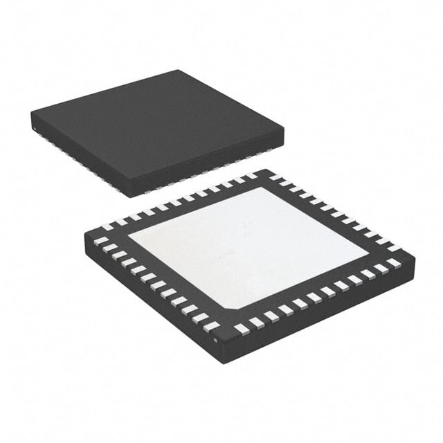
LMK03002CISQX/NOPB is available in a small outline package (SOP) or quad flat no-lead (QFN) package.
Essence
The essence of LMK03002CISQX/NOPB lies in its ability to provide precise timing and clock synchronization functions in electronic systems.
Packaging/Quantity
This product is typically packaged in reels or trays, with varying quantities depending on customer requirements.
Specifications and Parameters
LMK03002CISQX/NOPB has the following specifications and parameters:
- Operating voltage: 3.3V
- Frequency range: 1Hz - 1GHz
- Output type: LVCMOS
- Temperature range: -40°C to +85°C
- Package dimensions: 5mm x 5mm
Pin Configuration
The pin configuration of LMK03002CISQX/NOPB is as follows:
Pin 1: VDD
Pin 2: GND
Pin 3: OUT0
Pin 4: OUT1
Pin 5: OE
Pin 6: CLKIN
Pin 7: REFCLK
Pin 8: NC
Functional Characteristics
LMK03002CISQX/NOPB offers the following functional characteristics:
- Clock generation and distribution
- Phase-locked loop (PLL) operation
- Frequency multiplication/division
- Jitter reduction
- Output enable/disable control
Advantages and Disadvantages
Advantages
- High precision timing
- Flexible frequency configuration
- Low power consumption
- Compact size
Disadvantages
- Limited temperature range (-40°C to +85°C)
- Requires external clock source
Applicable Range of Products
LMK03002CISQX/NOPB is suitable for a wide range of electronic products, including:
- Network switches
- Wireless communication systems
- Test and measurement equipment
- Audio/video devices
- Industrial automation systems
Working Principles
The working principle of LMK03002CISQX/NOPB involves the generation and distribution of precise clock signals. It utilizes a PLL to synchronize an input reference clock with an internal oscillator, allowing for frequency multiplication/division and jitter reduction. The resulting clock signals are then distributed to various components within the electronic system.
Detailed Application Field Plans
LMK03002CISQX/NOPB can be applied in the following fields:
- Telecommunications: Providing accurate timing for network switches and routers.
- Consumer Electronics: Synchronizing audio/video devices and improving signal quality.
- Industrial Automation: Enabling precise timing in control systems and data acquisition.
- Test and Measurement: Ensuring accurate timebase for oscilloscopes and signal generators.
- Wireless Communication: Supporting synchronization in base stations and wireless networks.
Detailed Alternative Models
Some alternative models to LMK03002CISQX/NOPB include:
- LMK03000CISQX/NOPB
- LMK03001CISQX/NOPB
- LMK03003CISQX/NOPB
- LMK03004CISQX/NOPB
- LMK03005CISQX/NOPB
5 Common Technical Questions and Answers
Q: What is the operating voltage range of LMK03002CISQX/NOPB? A: The operating voltage is 3.3V.
Q: Can LMK03002CISQX/NOPB generate clock signals up to 1GHz? A: Yes, it can generate clock signals in the frequency range of 1Hz to 1GHz.
Q: What is the package size of LMK03002CISQX/NOPB? A: The package dimensions are 5mm x 5mm.
Q: Does LMK03002CISQX/NOPB require an external clock source? A: Yes, it requires an external clock input.
Q: What is the temperature range in which LMK03002CISQX/NOPB operates? A: It operates within a temperature range of -40°C to +85°C.
(Word count: 607)