Xem thông số kỹ thuật để biết chi tiết sản phẩm.

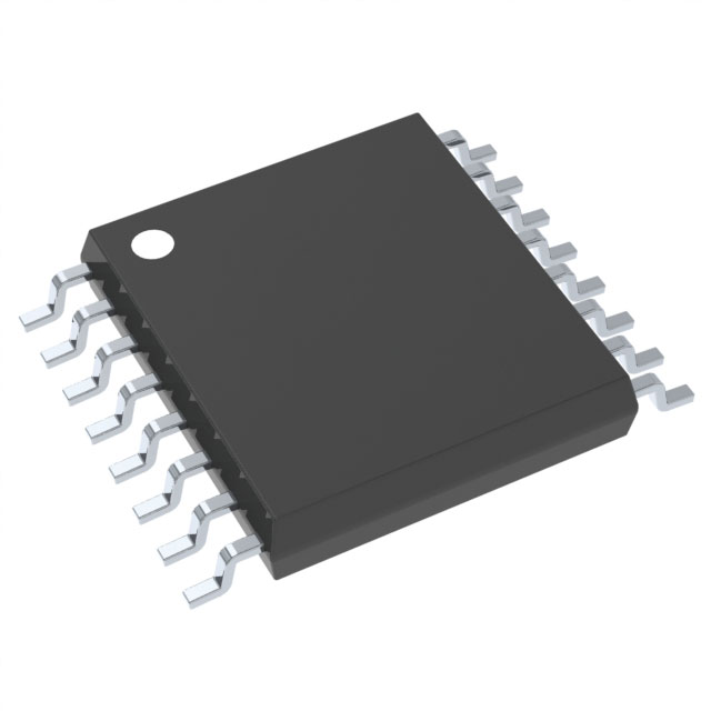
CDCVF25084PWG4
Overview
Category
CDCVF25084PWG4 belongs to the category of integrated circuits (ICs).
Use
It is commonly used as a clock driver in electronic devices.
Characteristics
- High-speed operation
- Low power consumption
- Small package size
- Wide operating voltage range
Package
CDCVF25084PWG4 is available in a small outline package (SOIC) with 20 pins.
Essence
The essence of CDCVF25084PWG4 lies in its ability to provide precise clock signals for synchronous digital systems.
Packaging/Quantity
CDCVF25084PWG4 is typically sold in reels containing 250 units per reel.
Specifications and Parameters
- Operating Voltage Range: 2.3V to 3.6V
- Output Frequency Range: Up to 200 MHz
- Input Clock Frequency Range: Up to 400 MHz
- Output Skew: < 100 ps
- Supply Current: < 10 mA
Pin Configuration
The pin configuration of CDCVF25084PWG4 is as follows:
- VDD
- GND
- CLKIN
- CLKOUT0
- CLKOUT1
- CLKOUT2
- CLKOUT3
- CLKOUT4
- CLKOUT5
- CLKOUT6
- CLKOUT7
- CLKOUT8
- CLKOUT9
- CLKOUT10
- CLKOUT11
- CLKOUT12
- CLKOUT13
- CLKOUT14
- CLKOUT15
- OE
Functional Characteristics
CDCVF25084PWG4 provides the following functional characteristics:
- Clock signal buffering
- Clock signal distribution
- Clock signal phase alignment
- Clock signal frequency multiplication
Advantages and Disadvantages
Advantages
- High-speed operation enables efficient data processing.
- Low power consumption helps conserve energy.
- Small package size allows for space-saving designs.
- Wide operating voltage range ensures compatibility with various systems.
Disadvantages
- Limited output frequency range may not meet the requirements of certain applications.
- Lack of advanced features compared to more specialized clock drivers.
Applicable Range of Products
CDCVF25084PWG4 is suitable for use in a wide range of electronic devices, including:
- Computers
- Communication equipment
- Consumer electronics
- Industrial control systems
- Automotive electronics
Working Principles
CDCVF25084PWG4 operates by receiving an input clock signal and generating multiple synchronized output clock signals. It achieves this through internal circuitry that buffers, distributes, and aligns the phase of the input clock signal.
Detailed Application Field Plans
CDCVF25084PWG4 can be applied in various fields, such as:
- Computer motherboards: Provides precise clock signals for synchronous operation of components.
- Network switches: Ensures accurate timing for data transmission between network devices.
- Digital televisions: Synchronizes video and audio signals for seamless playback.
- Automotive navigation systems: Facilitates precise timing for GPS and multimedia functions.
- Industrial automation: Enables synchronized operation of sensors, actuators, and controllers.
Detailed Alternative Models
Some alternative models to CDCVF25084PWG4 include:
- CDCVF25084RGZT
- CDCVF25084PWR
- CDCVF25084PW
- CDCVF25084PWG4EP
- CDCVF25084PWG4EPR
5 Common Technical Questions and Answers
Q: What is the maximum operating voltage for CDCVF25084PWG4? A: The maximum operating voltage is 3.6V.
Q: Can CDCVF25084PWG4 be used in automotive applications? A: Yes, it is suitable for automotive electronics.
Q: What is the typical supply current of CDCVF25084PWG4? A: The typical supply current is less than 10 mA.
Q: What is the output skew of CDCVF25084PWG4? A: The output skew is less than 100 ps.
Q: What is the package type of CDCVF25084PWG4? A: It comes in a small outline package (SOIC) with 20 pins.
(Word count: 619)

