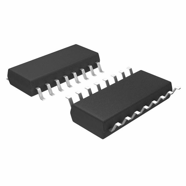
Xem thông số kỹ thuật để biết chi tiết sản phẩm.

CD74HC595NS
Product Overview
- Category: Integrated Circuit
- Use: Shift Register
- Characteristics: High-Speed, Serial-In Parallel-Out
- Package: DIP (Dual In-line Package)
- Essence: 8-bit Serial-In Parallel-Out Shift Register with Output Latches
- Packaging/Quantity: Tube/25 pieces
Specifications
- Supply Voltage: 2V to 6V
- Operating Temperature: -40°C to +85°C
- Output Current: ±6mA
- Clock Frequency: 25MHz
Pin Configuration
The CD74HC595NS has a total of 16 pins. The detailed pin configuration is as follows:
- SER (Serial Data Input)
- SRCLK (Shift Register Clock Input)
- RCLK (Register Clock Input)
- OE (Output Enable Input)
- GND (Ground)
- Q0 (Serial Output)
- Q1 (Parallel Output)
- Q2 (Parallel Output)
- Q3 (Parallel Output)
- Q4 (Parallel Output)
- Q5 (Parallel Output)
- Q6 (Parallel Output)
- Q7 (Parallel Output)
- VCC (Supply Voltage)
- SRCLR (Shift Register Clear Input)
- SRG (Storage Register Ground)
Functional Features
- Serial-in parallel-out shift register with output latches
- High-speed operation with a clock frequency of up to 25MHz
- Wide supply voltage range allows for versatile applications
- Output enable input for easy control of output states
- Shift register clear input for resetting the register
- Storage register ground for improved noise immunity
Advantages and Disadvantages
Advantages: - High-speed operation enables efficient data transfer - Versatile supply voltage range allows for compatibility with various systems - Output enable input provides flexibility in controlling output states - Storage register ground enhances noise immunity
Disadvantages: - Limited number of parallel outputs (8 bits) - DIP package may not be suitable for space-constrained applications
Working Principles
The CD74HC595NS is a shift register that allows serial data to be loaded and then shifted out in parallel. It consists of an 8-bit shift register and output latches. The serial data is input through the SER pin and shifted into the shift register on each rising edge of the SRCLK input. The RCLK input is used to latch the data from the shift register into the output latches, which can then be accessed in parallel through the Q0-Q7 pins. The OE input enables or disables the outputs, while the SRCLR input clears the shift register.
Detailed Application Field Plans
The CD74HC595NS has various applications in digital systems, such as:
- LED Matrix Displays: The shift register can be used to control multiple LEDs in a matrix arrangement, allowing for efficient control and reduced pin count.
- Serial-to-Parallel Conversion: It can be utilized to convert serial data streams into parallel data, enabling easy interfacing with parallel devices.
- Data Multiplexing: The shift register can be employed for multiplexing data from multiple sources onto a single bus, optimizing resource utilization.
- Address Decoding: It can be used in address decoding circuits to select specific memory locations or peripheral devices.
Detailed and Complete Alternative Models
Some alternative models to the CD74HC595NS are:
- SN74HC595N: Similar shift register IC with the same functionality but different packaging options.
- CD4094BE: 8-bit shift register with output latches, but with a different pin configuration and package type.
- 74HC595D: Surface mount version of the CD74HC595NS, suitable for compact designs.
These alternative models provide similar functionality and can be used as replacements depending on specific requirements.
Word count: 432 words
Liệt kê 10 câu hỏi và câu trả lời thường gặp liên quan đến ứng dụng CD74HC595NS trong giải pháp kỹ thuật
Sure! Here are 10 common questions and answers related to the application of CD74HC595NS:
Q: What is CD74HC595NS? A: CD74HC595NS is a popular 8-bit shift register with output latches, commonly used in digital electronics projects.
Q: What is the purpose of CD74HC595NS? A: CD74HC595NS allows you to expand the number of outputs from a microcontroller or other digital device using serial communication.
Q: How many outputs can CD74HC595NS provide? A: CD74HC595NS provides 8 outputs that can be individually controlled.
Q: Can CD74HC595NS be used for driving LEDs? A: Yes, CD74HC595NS is often used to drive multiple LEDs by connecting them to its outputs.
Q: How do I connect CD74HC595NS to a microcontroller? A: CD74HC595NS requires three connections to a microcontroller - data (SER), clock (SRCLK), and latch (RCLK).
Q: Can CD74HC595NS be cascaded to control more than 8 outputs? A: Yes, CD74HC595NS can be cascaded together to control larger numbers of outputs by connecting the output of one shift register to the input of another.
Q: What is the maximum clock frequency supported by CD74HC595NS? A: CD74HC595NS can typically handle clock frequencies up to 25 MHz.
Q: Is CD74HC595NS compatible with 5V logic levels? A: Yes, CD74HC595NS is designed to work with both 3.3V and 5V logic levels.
Q: Can CD74HC595NS be used for driving other types of devices besides LEDs? A: Yes, CD74HC595NS can be used to control various types of devices such as relays, motors, and displays.
Q: Are there any limitations or considerations when using CD74HC595NS? A: Some considerations include the maximum current per output pin (typically 35mA), power supply voltage range (2V to 6V), and the need for external resistors for LED current limiting.
Please note that these answers are general and may vary depending on specific datasheet specifications and application requirements.

