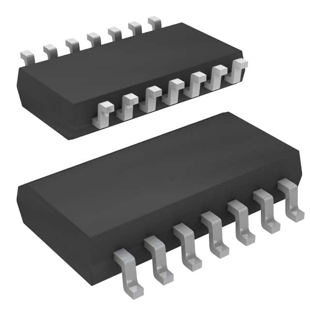
Xem thông số kỹ thuật để biết chi tiết sản phẩm.

CD74HC4075NSR
Product Overview
- Category: Integrated Circuit (IC)
- Use: Logic Gate
- Characteristics: High-Speed CMOS, Triple 3-Input OR Gate
- Package: SOIC-14
- Essence: The CD74HC4075NSR is a logic gate IC that performs the OR operation on three input signals.
- Packaging/Quantity: The CD74HC4075NSR is typically sold in reels of 2500 units.
Specifications
- Supply Voltage Range: 2V to 6V
- Logic Family: HC
- Number of Inputs: 3
- Number of Outputs: 1
- Propagation Delay: 9 ns (typical)
- Operating Temperature Range: -40°C to +85°C
Detailed Pin Configuration
The CD74HC4075NSR has a total of 14 pins. The pin configuration is as follows:
__    __
   A1 |1  \__/ 14| VCC
   A2 |2        13| C
   B1 |3        12| B
   B2 |4   CD   11| A
   B3 |5   74   10| GND
   Y1 |6   HC   9 | Y
   Y2 |7        8 | Y3
       --        --
Functional Features
- Performs the OR operation on three input signals (A, B, and C).
- Provides a single output signal (Y) based on the logical OR of the inputs.
- High-speed operation due to the CMOS technology used.
- Wide supply voltage range allows for flexibility in various applications.
- Low power consumption.
Advantages and Disadvantages
Advantages
- High-speed operation enables efficient processing of logic operations.
- Wide supply voltage range allows for compatibility with different systems.
- Low power consumption helps in reducing overall energy usage.
Disadvantages
- Limited number of inputs and outputs restricts the complexity of logic functions that can be implemented.
- The SOIC-14 package may not be suitable for all applications, especially those requiring smaller form factors.
Working Principles
The CD74HC4075NSR is based on CMOS technology, which utilizes both NMOS and PMOS transistors to implement logic gates. In this particular IC, three input signals (A, B, and C) are fed into the OR gate circuitry. The internal circuitry performs the logical OR operation on these inputs and generates a single output signal (Y). The propagation delay of 9 ns (typical) ensures fast response times.
Detailed Application Field Plans
The CD74HC4075NSR can be used in various applications where logical OR operations are required. Some potential application fields include:
- Digital electronics: The IC can be used in digital circuits to combine multiple input signals and generate an output based on their logical OR combination.
- Data processing: It can be utilized in data processing systems to perform logical operations on binary data.
- Communication systems: The IC can be employed in communication systems to process incoming signals and determine the presence of specific conditions.
Detailed and Complete Alternative Models
There are several alternative models available that offer similar functionality to the CD74HC4075NSR. Some notable alternatives include:
- SN74HC4075: This IC from Texas Instruments offers the same triple 3-input OR gate functionality in a DIP-14 package.
- MC74HC4075: Manufactured by ON Semiconductor, this IC also provides triple 3-input OR gate functionality but comes in a TSSOP-14 package.
- CD4075: This IC from Texas Instruments is a non-inverting version of the triple 3-input OR gate, available in a DIP-14 package.
These alternative models can be considered based on specific requirements such as package type, manufacturer preference, or availability.
In conclusion, the CD74HC4075NSR is a high-speed CMOS logic gate IC that performs the OR operation on three input signals. It offers advantages such as fast operation, wide supply voltage range, and low power consumption. However, it has limitations in terms of the number of inputs and outputs. The IC finds applications in digital electronics, data processing, and communication systems. Alternative models like SN74HC4075, MC74HC4075, and CD4075 provide similar functionality with variations in package type and manufacturer.
Liệt kê 10 câu hỏi và câu trả lời thường gặp liên quan đến ứng dụng CD74HC4075NSR trong giải pháp kỹ thuật
Sure! Here are 10 common questions and answers related to the application of CD74HC4075NSR in technical solutions:
Q: What is CD74HC4075NSR? A: CD74HC4075NSR is a quad 2-input OR gate integrated circuit (IC) that can be used in various digital logic applications.
Q: What is the operating voltage range of CD74HC4075NSR? A: CD74HC4075NSR operates within a voltage range of 2V to 6V.
Q: What is the maximum output current of CD74HC4075NSR? A: The maximum output current of CD74HC4075NSR is typically around 5.2mA.
Q: Can CD74HC4075NSR be used for level shifting applications? A: Yes, CD74HC4075NSR can be used for level shifting as it supports both TTL and CMOS logic levels.
Q: What is the typical propagation delay of CD74HC4075NSR? A: The typical propagation delay of CD74HC4075NSR is around 9ns.
Q: Is CD74HC4075NSR suitable for high-speed applications? A: Yes, CD74HC4075NSR is designed for high-speed operation and can be used in applications requiring fast switching times.
Q: Can CD74HC4075NSR be used in battery-powered devices? A: Yes, CD74HC4075NSR has a low power consumption and can be used in battery-powered devices.
Q: Does CD74HC4075NSR have built-in protection against electrostatic discharge (ESD)? A: Yes, CD74HC4075NSR has built-in ESD protection, making it more robust against static electricity.
Q: Can CD74HC4075NSR be used in temperature-sensitive applications? A: Yes, CD74HC4075NSR has a wide operating temperature range of -40°C to 85°C, making it suitable for various environments.
Q: What is the package type of CD74HC4075NSR? A: CD74HC4075NSR is available in a small-outline integrated circuit (SOIC) package with 14 pins.
Please note that these answers are general and may vary depending on specific datasheet specifications.

