Xem thông số kỹ thuật để biết chi tiết sản phẩm.

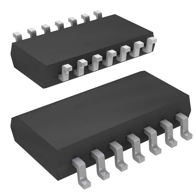
CD74HC4002NSRG4
Product Overview
- Category: Integrated Circuit
- Use: Logic Gates
- Characteristics: High-Speed CMOS, Quad 2-Input NOR Gate
- Package: SOIC-14
- Essence: The CD74HC4002NSRG4 is a quad 2-input NOR gate that operates at high-speed using CMOS technology.
- Packaging/Quantity: Available in reels of 2500 units.
Specifications
- Supply Voltage: 2V to 6V
- Logic Family: HC
- Number of Inputs: 2
- Number of Gates: 4
- Propagation Delay: 9 ns (typical)
- Operating Temperature Range: -40°C to +85°C
Detailed Pin Configuration
The CD74HC4002NSRG4 has a total of 14 pins. The pin configuration is as follows:
- A Input 1
- B Input 1
- Y Output 1
- GND (Ground)
- Y Output 2
- B Input 2
- A Input 2
- VCC (Supply Voltage)
- Y Output 3
- B Input 3
- A Input 3
- Y Output 4
- B Input 4
- A Input 4
Functional Features
- High-Speed Operation: The CD74HC4002NSRG4 offers fast switching speeds, making it suitable for applications requiring quick response times.
- Wide Supply Voltage Range: It can operate within a supply voltage range of 2V to 6V, providing flexibility in various electronic systems.
- Low Power Consumption: This IC consumes low power, making it energy-efficient and suitable for battery-powered devices.
- Noise Immunity: The CMOS technology used in the CD74HC4002NSRG4 provides excellent noise immunity, ensuring reliable operation even in noisy environments.
Advantages and Disadvantages
Advantages: - High-speed operation - Wide supply voltage range - Low power consumption - Excellent noise immunity
Disadvantages: - Limited number of gates (4) - Not suitable for high-voltage applications
Working Principles
The CD74HC4002NSRG4 is based on CMOS technology, which utilizes both NMOS and PMOS transistors to achieve high-speed operation. The NOR gate performs logical OR operation on its inputs and produces a low output only when all inputs are high. It operates by switching the internal transistors on or off based on the input signals, resulting in the desired logic function.
Detailed Application Field Plans
The CD74HC4002NSRG4 can be used in various applications, including:
- Digital Logic Circuits: It can be used as a building block for designing complex digital systems such as microprocessors, memory units, and arithmetic circuits.
- Data Processing: The NOR gate's logical OR operation makes it suitable for data processing tasks like error detection, parity checking, and data manipulation.
- Signal Conditioning: It can be used to condition and process analog signals before converting them into digital form.
- Control Systems: The CD74HC4002NSRG4 can be employed in control systems to implement logical functions required for decision-making and control operations.
Detailed and Complete Alternative Models
- SN74HC02N: Quad 2-Input NOR Gate, DIP-14 package
- MC74HC02AN: Quad 2-Input NOR Gate, PDIP-14 package
- CD4002BE: Dual 4-Input NOR Gate, DIP-14 package
- 74HCT02N: Quad 2-Input NOR Gate, DIP-14 package
These alternative models offer similar functionality and can be used as substitutes for the CD74HC4002NSRG4 in various applications.
In conclusion, the CD74HC4002NSRG4 is a high-speed CMOS quad 2-input NOR gate that offers excellent noise immunity and low power consumption. It is widely used in digital logic circuits, data processing, signal conditioning, and control systems. Alternative models are available to suit different requirements and preferences.
Liệt kê 10 câu hỏi và câu trả lời thường gặp liên quan đến ứng dụng CD74HC4002NSRG4 trong giải pháp kỹ thuật
Sure! Here are 10 common questions and answers related to the application of CD74HC4002NSRG4:
Q: What is CD74HC4002NSRG4? A: CD74HC4002NSRG4 is a quad 2-input NOR gate IC (integrated circuit) that is commonly used in digital logic applications.
Q: What is the operating voltage range for CD74HC4002NSRG4? A: The operating voltage range for CD74HC4002NSRG4 is typically between 2V and 6V.
Q: What is the maximum output current of CD74HC4002NSRG4? A: The maximum output current of CD74HC4002NSRG4 is around 5.2mA.
Q: Can CD74HC4002NSRG4 be used in high-speed applications? A: Yes, CD74HC4002NSRG4 is designed for high-speed operation and can be used in various high-frequency applications.
Q: What is the typical propagation delay of CD74HC4002NSRG4? A: The typical propagation delay of CD74HC4002NSRG4 is around 9ns.
Q: Is CD74HC4002NSRG4 compatible with both CMOS and TTL logic levels? A: Yes, CD74HC4002NSRG4 is compatible with both CMOS (Complementary Metal-Oxide-Semiconductor) and TTL (Transistor-Transistor Logic) logic levels.
Q: Can CD74HC4002NSRG4 be used as a buffer or an inverter? A: No, CD74HC4002NSRG4 is specifically designed as a quad 2-input NOR gate and cannot be used as a buffer or an inverter.
Q: What is the maximum operating temperature for CD74HC4002NSRG4? A: The maximum operating temperature for CD74HC4002NSRG4 is typically around 125°C.
Q: Can CD74HC4002NSRG4 drive capacitive loads directly? A: Yes, CD74HC4002NSRG4 can drive small capacitive loads directly without requiring additional buffering.
Q: Are there any recommended decoupling capacitors for CD74HC4002NSRG4? A: It is generally recommended to use a 0.1µF ceramic capacitor placed close to the power supply pins of CD74HC4002NSRG4 for proper decoupling.
Please note that these answers are general and may vary depending on specific application requirements. Always refer to the datasheet and consult with technical experts for accurate information.

