

Xem thông số kỹ thuật để biết chi tiết sản phẩm.
ADS42LB49IRGC25
Product Overview
Category
The ADS42LB49IRGC25 belongs to the category of integrated circuits (ICs).
Use
This product is primarily used in electronic devices for signal processing and data conversion.
Characteristics
- High-speed data conversion
- Low power consumption
- Compact size
- Wide operating temperature range
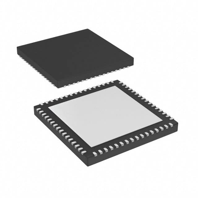
Package
The ADS42LB49IRGC25 is available in a small form factor package, which ensures easy integration into various electronic systems.
Essence
The essence of this product lies in its ability to accurately convert analog signals into digital format, enabling efficient signal processing and analysis.
Packaging/Quantity
The ADS42LB49IRGC25 is typically packaged in reels or trays, with a quantity of 250 units per reel/tray.
Specifications
- Resolution: 16 bits
- Sampling Rate: Up to 250 Mega Samples Per Second (MSPS)
- Input Voltage Range: ±2 V
- Power Supply: 3.3 V
- Operating Temperature Range: -40°C to +85°C
Detailed Pin Configuration
- VDDA: Analog power supply
- VDDD: Digital power supply
- VINP: Positive analog input
- VINN: Negative analog input
- REFOUT: Reference voltage output
- CLKIN: Clock input
- CLKOUT: Clock output
- D[15:0]: Digital output data bus
- FS: Frame synchronization input
- CS: Chip select input
- RESET: Reset input
- GND: Ground
Functional Features
- High-speed analog-to-digital conversion
- Programmable gain amplifier
- Built-in reference voltage generator
- Flexible clocking options
- Serial interface for easy integration with microcontrollers or digital signal processors
Advantages and Disadvantages
Advantages
- High-resolution conversion for accurate signal representation
- Low power consumption for energy-efficient operation
- Compact size allows for space-saving integration
- Wide operating temperature range enables usage in various environments
Disadvantages
- Limited input voltage range may require additional signal conditioning circuitry in some applications
- Higher cost compared to lower-end analog-to-digital converters
Working Principles
The ADS42LB49IRGC25 utilizes a successive approximation register (SAR) architecture to convert analog signals into digital format. It employs a combination of sample-and-hold, amplification, and quantization techniques to accurately capture and digitize the input signal.
Detailed Application Field Plans
The ADS42LB49IRGC25 finds application in various fields, including:
- Communications: Used in wireless communication systems for baseband signal processing.
- Test and Measurement: Enables high-speed data acquisition and analysis in test equipment.
- Medical Devices: Utilized in medical imaging systems for precise signal conversion.
- Industrial Automation: Enables accurate data acquisition and control in industrial monitoring systems.
Detailed and Complete Alternative Models
- ADS42LB69IRGC25: Similar to ADS42LB49IRGC25 but with higher resolution (18 bits).
- ADS42LB99IRGC25: Similar to ADS42LB49IRGC25 but with higher sampling rate (500 MSPS).
- ADS42LB29IRGC25: Similar to ADS42LB49IRGC25 but with lower power consumption.
These alternative models provide options with varying specifications to cater to different application requirements.
Word count: 489 words
Liệt kê 10 câu hỏi và câu trả lời thường gặp liên quan đến ứng dụng ADS42LB49IRGC25 trong giải pháp kỹ thuật
Sure! Here are 10 common questions and answers related to the application of ADS42LB49IRGC25 in technical solutions:
Q: What is the ADS42LB49IRGC25? A: The ADS42LB49IRGC25 is a high-performance analog-to-digital converter (ADC) designed for applications that require high-speed data acquisition.
Q: What is the maximum sampling rate of the ADS42LB49IRGC25? A: The ADS42LB49IRGC25 can achieve a maximum sampling rate of 250 MSPS (Mega Samples Per Second).
Q: What is the resolution of the ADC? A: The ADS42LB49IRGC25 has a resolution of 14 bits, which means it can represent analog signals with 2^14 (16,384) discrete levels.
Q: What is the input voltage range of the ADC? A: The ADS42LB49IRGC25 has a differential input voltage range of ±0.5 V.
Q: Can the ADC operate in single-ended mode? A: No, the ADS42LB49IRGC25 is a differential ADC and requires differential input signals.
Q: What is the power supply voltage range for the ADC? A: The ADS42LB49IRGC25 operates from a single power supply voltage ranging from 1.8 V to 3.3 V.
Q: Does the ADC support various digital output formats? A: Yes, the ADS42LB49IRGC25 supports various digital output formats including LVDS (Low Voltage Differential Signaling) and CMOS.
Q: Is there any built-in digital signal processing (DSP) functionality in the ADC? A: No, the ADS42LB49IRGC25 is a standalone ADC and does not have built-in DSP functionality. However, it can be used in conjunction with external DSP devices.
Q: What are some typical applications of the ADS42LB49IRGC25? A: The ADS42LB49IRGC25 is commonly used in applications such as wireless communication systems, radar systems, medical imaging, and test and measurement equipment.
Q: Are there evaluation boards or development kits available for the ADC? A: Yes, Texas Instruments provides evaluation boards and development kits for the ADS42LB49IRGC25, which can help engineers quickly prototype and evaluate their designs.
Please note that these answers are general and may vary depending on the specific requirements and use cases of the application.