

Xem thông số kỹ thuật để biết chi tiết sản phẩm.
ADC10065CIMTX/NOPB
Product Overview
- Category: Analog-to-Digital Converter (ADC)
- Use: Converts analog signals into digital data for processing and analysis
- Characteristics:
- High resolution and accuracy
- Fast conversion speed
- Low power consumption
- Package: CIMTX
- Essence: Provides precise digital representation of analog signals
- Packaging/Quantity: Available in tape and reel packaging, quantity varies based on supplier
Specifications
- Resolution: 10 bits
- Conversion Rate: 100 kilosamples per second (ksps)
- Input Voltage Range: 0 to Vref
- Power Supply: 2.7V to 5.5V
- Operating Temperature Range: -40°C to +85°C
- Interface: Serial Peripheral Interface (SPI)
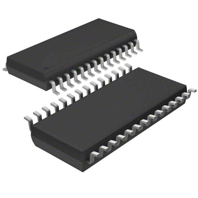
Pin Configuration
The ADC10065CIMTX/NOPB has the following pin configuration:
- VDD: Power supply voltage
- VREF: Reference voltage input
- AGND: Analog ground
- VIN: Analog input voltage
- CLK: Clock input
- CS: Chip select input
- DOUT: Digital output
- DGND: Digital ground
Functional Features
- High-resolution conversion with 10-bit accuracy
- Fast conversion rate of 100 ksps
- Low power consumption for energy-efficient operation
- SPI interface for easy integration with microcontrollers and other digital systems
- Wide operating temperature range for versatile applications
Advantages and Disadvantages
Advantages: - High resolution and accuracy ensure precise signal conversion - Fast conversion rate allows for real-time data acquisition - Low power consumption reduces energy usage and extends battery life - SPI interface simplifies communication with other devices - Wide operating temperature range enables usage in various environments
Disadvantages: - Limited resolution compared to higher-bit ADCs - Lower conversion rate compared to some high-speed ADCs - Requires external reference voltage for accurate conversions
Working Principles
The ADC10065CIMTX/NOPB operates based on the successive approximation method. It samples the analog input voltage and compares it with a reference voltage. By iteratively adjusting the digital representation of the input voltage, it converges to a digital value that closely represents the analog signal.
Detailed Application Field Plans
The ADC10065CIMTX/NOPB finds applications in various fields, including:
- Industrial Automation: Used for data acquisition in control systems, process monitoring, and equipment diagnostics.
- Medical Devices: Enables precise measurement and analysis of physiological signals in medical instruments.
- Automotive Electronics: Utilized in vehicle diagnostics, sensor data processing, and engine control systems.
- Communications: Supports signal processing in wireless communication systems, base stations, and network analyzers.
- Test and Measurement: Provides accurate data acquisition in oscilloscopes, spectrum analyzers, and data loggers.
Detailed and Complete Alternative Models
- ADC10154CIMT/NOPB: 10-bit ADC with similar characteristics and package.
- ADC12062CIMT/NOPB: 12-bit ADC with higher resolution and similar package.
- ADC08080CIMT/NOPB: 8-bit ADC with lower resolution and similar package.
- ADC14155CIMT/NOPB: 14-bit ADC with higher resolution and similar package.
- ADC06032CIMT/NOPB: 6-bit ADC with lower resolution and similar package.
(Note: The above alternative models are provided as examples and may not be an exhaustive list.)
Word count: 342 words
Liệt kê 10 câu hỏi và câu trả lời thường gặp liên quan đến ứng dụng ADC10065CIMTX/NOPB trong giải pháp kỹ thuật
Sure! Here are 10 common questions and answers related to the application of ADC10065CIMTX/NOPB in technical solutions:
Q: What is the ADC10065CIMTX/NOPB? A: The ADC10065CIMTX/NOPB is a high-speed, low-power analog-to-digital converter (ADC) integrated circuit.
Q: What is the resolution of the ADC10065CIMTX/NOPB? A: The ADC10065CIMTX/NOPB has a resolution of 10 bits, meaning it can represent analog signals with 2^10 (1024) discrete levels.
Q: What is the maximum sampling rate of the ADC10065CIMTX/NOPB? A: The ADC10065CIMTX/NOPB has a maximum sampling rate of 100 Mega-samples per second (MSPS).
Q: What is the power supply voltage range for the ADC10065CIMTX/NOPB? A: The ADC10065CIMTX/NOPB operates with a power supply voltage range of 2.7V to 5.5V.
Q: What is the typical power consumption of the ADC10065CIMTX/NOPB? A: The typical power consumption of the ADC10065CIMTX/NOPB is around 50 milliwatts (mW).
Q: What is the input voltage range of the ADC10065CIMTX/NOPB? A: The ADC10065CIMTX/NOPB has a differential input voltage range of -0.3V to VREF+0.3V.
Q: Does the ADC10065CIMTX/NOPB have built-in reference voltage? A: No, the ADC10065CIMTX/NOPB requires an external reference voltage for its operation.
Q: What is the output interface of the ADC10065CIMTX/NOPB? A: The ADC10065CIMTX/NOPB has a parallel CMOS/TTL-compatible output interface.
Q: Can the ADC10065CIMTX/NOPB be used in battery-powered applications? A: Yes, the low power consumption and wide power supply voltage range make it suitable for battery-powered applications.
Q: What are some typical applications of the ADC10065CIMTX/NOPB? A: The ADC10065CIMTX/NOPB can be used in various applications such as communications, medical imaging, test and measurement equipment, and industrial automation.
Please note that these answers are general and may vary depending on specific implementation requirements and datasheet specifications.