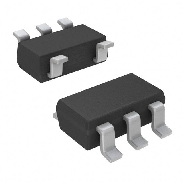
Xem thông số kỹ thuật để biết chi tiết sản phẩm.

Encyclopedia Entry: 74LVC1G125DCKTG4
Product Overview
- Category: Integrated Circuit (IC)
- Use: Logic Level Shifter
- Characteristics: Low-voltage, high-speed, single gate buffer
- Package: DCKT (SC-70-5), Tape and Reel
- Essence: Buffering and level shifting signals in low-voltage applications
- Packaging/Quantity: 3000 units per reel
Specifications
- Supply Voltage Range: 1.65V to 5.5V
- High-Level Input Voltage: 0.7 x VCC
- Low-Level Input Voltage: 0.3 x VCC
- High-Level Output Voltage: 0.9 x VCC
- Low-Level Output Voltage: 0.1 x VCC
- Maximum Operating Frequency: 400 MHz
- Propagation Delay: 2.8 ns (typical)
Detailed Pin Configuration
The 74LVC1G125DCKTG4 has a total of 5 pins: 1. GND (Ground): Connected to the ground reference of the circuit. 2. A (Input): Signal input pin. 3. OE (Output Enable): Controls the output buffer. 4. Y (Output): Buffered signal output pin. 5. VCC (Power Supply): Connected to the positive supply voltage.
Functional Features
- Single gate buffer with tri-state output.
- Provides level shifting between different voltage domains.
- Supports bidirectional data flow.
- High-speed operation suitable for various applications.
- Low power consumption.
- Schmitt-trigger input allows for noise immunity.
Advantages
- Compact size and low power consumption make it ideal for portable devices.
- Wide supply voltage range enables compatibility with different systems.
- Tri-state output allows for easy bus sharing and multiplexing.
- High-speed operation ensures efficient signal transmission.
- Schmitt-trigger input enhances noise immunity.
Disadvantages
- Limited number of gates in a single package.
- Not suitable for high-voltage applications.
- May require additional components for certain circuit configurations.
Working Principles
The 74LVC1G125DCKTG4 is a logic level shifter that operates as a single gate buffer. It takes an input signal and provides a buffered output signal at a different voltage level. The tri-state output allows the buffer to be disabled, effectively disconnecting the output pin from the circuit. This feature enables bus sharing and multiplexing.
The IC operates within a wide supply voltage range, making it compatible with various low-voltage systems. It utilizes a Schmitt-trigger input, which provides hysteresis and improves noise immunity by reducing the effects of signal fluctuations.
Detailed Application Field Plans
The 74LVC1G125DCKTG4 finds applications in various fields, including: 1. Portable Electronics: Used for level shifting and buffering signals in smartphones, tablets, and wearable devices. 2. Industrial Automation: Enables communication between different voltage domains in control systems and sensors. 3. Automotive Electronics: Facilitates signal translation and buffering in automotive control units and infotainment systems. 4. IoT Devices: Supports bidirectional data flow and level shifting in smart home devices and sensor networks.
Alternative Models (Detailed and Complete)
- SN74LVC1G125DBVR: SOT-23-5 package, Tape and Reel packaging, similar specifications.
- MC74LVC1G125DR2G: SOT-23-5 package, Tape and Reel packaging, comparable performance.
- TC7SZ125FU: SC-88A package, Tape and Reel packaging, equivalent functionality.
Note: The above alternative models are provided as examples and may have slight variations in specifications and packaging.
In conclusion, the 74LVC1G125DCKTG4 is a versatile logic level shifter and buffer IC. Its compact size, low power consumption, and high-speed operation make it suitable for various low-voltage applications. With its tri-state output and wide supply voltage range, it offers flexibility and compatibility. However, it has limitations in terms of gate count and high-voltage applications.
Liệt kê 10 câu hỏi và câu trả lời thường gặp liên quan đến ứng dụng 74LVC1G125DCKTG4 trong giải pháp kỹ thuật
Sure! Here are 10 common questions and answers related to the application of 74LVC1G125DCKTG4 in technical solutions:
Q1: What is the 74LVC1G125DCKTG4? A1: The 74LVC1G125DCKTG4 is a single bus buffer gate with 3-state output, designed for low-voltage (1.65V to 5.5V) applications.
Q2: What is the purpose of the 74LVC1G125DCKTG4? A2: The purpose of this IC is to provide buffering and level shifting capabilities in digital circuits.
Q3: What are the key features of the 74LVC1G125DCKTG4? A3: Some key features include wide operating voltage range, high-speed operation, 3-state outputs, and compatibility with various logic families.
Q4: How can I use the 74LVC1G125DCKTG4 for level shifting? A4: You can connect the input of the IC to a lower voltage level signal and the output to a higher voltage level signal, effectively shifting the logic levels.
Q5: Can I use the 74LVC1G125DCKTG4 as a voltage translator? A5: Yes, the IC can be used as a voltage translator between different voltage domains in mixed-voltage systems.
Q6: What is the maximum operating frequency of the 74LVC1G125DCKTG4? A6: The maximum operating frequency is typically around 400 MHz.
Q7: Can I use the 74LVC1G125DCKTG4 in battery-powered applications? A7: Yes, the IC is suitable for battery-powered applications due to its low power consumption and wide operating voltage range.
Q8: Is the 74LVC1G125DCKTG4 compatible with other logic families? A8: Yes, it is compatible with various logic families such as TTL, CMOS, and LVCMOS.
Q9: Can I use the 74LVC1G125DCKTG4 for bidirectional level shifting? A9: No, the IC is unidirectional and can only shift levels in one direction.
Q10: What is the package type of the 74LVC1G125DCKTG4? A10: The IC comes in a small SOT-23-5 package, which is suitable for space-constrained applications.
Please note that these answers are general and may vary depending on specific application requirements.

