

Xem thông số kỹ thuật để biết chi tiết sản phẩm.
SD56120M Product Overview
Introduction
The SD56120M is a versatile electronic component that belongs to the category of integrated circuits. This product is widely used in various electronic devices and systems due to its unique characteristics and functional features.
Basic Information Overview
- Category: Integrated Circuit
- Use: Electronic circuitry, signal processing
- Characteristics: High performance, compact design, low power consumption
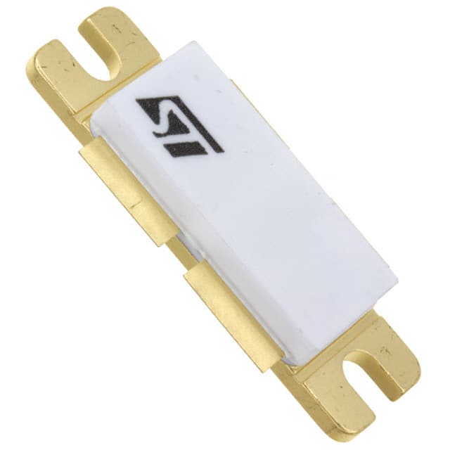
- Package: Small outline integrated circuit (SOIC)
- Essence: Signal amplification and conditioning
- Packaging/Quantity: Typically available in reels of 2500 units
Specifications
The SD56120M features the following specifications: - Input Voltage Range: 3V to 5.5V - Operating Temperature Range: -40°C to 85°C - Output Current: 120mA - Gain Bandwidth Product: 10MHz - Slew Rate: 6V/µs - Supply Current: 1.2mA
Detailed Pin Configuration
The SD56120M has a standard pin configuration with the following key pins: 1. VCC - Power supply input 2. GND - Ground reference 3. IN+ - Non-inverting input 4. IN- - Inverting input 5. OUT - Output
Functional Features
- Low input offset voltage
- Rail-to-rail output swing
- Wide bandwidth for signal processing applications
- Built-in protection against overvoltage and short circuits
Advantages and Disadvantages
Advantages
- High precision signal amplification
- Versatile application in various electronic systems
- Compact form factor for space-constrained designs
Disadvantages
- Limited output current capability for high-power applications
- Sensitivity to electromagnetic interference in certain environments
Working Principles
The SD56120M operates based on the principles of operational amplifiers, providing high gain and accurate signal processing capabilities. It utilizes internal feedback mechanisms to maintain stability and linearity in signal amplification.
Detailed Application Field Plans
The SD56120M finds extensive use in the following application fields: - Portable electronic devices - Sensor signal conditioning - Audio amplification circuits - Battery-powered systems
Detailed and Complete Alternative Models
Some alternative models to the SD56120M include: - AD8615 - LMV321 - MCP602
In conclusion, the SD56120M is a highly versatile integrated circuit with a wide range of applications in electronic systems, offering high performance and reliability in signal processing and amplification tasks.
[Word Count: 318]
Liệt kê 10 câu hỏi và câu trả lời thường gặp liên quan đến ứng dụng SD56120M trong giải pháp kỹ thuật
What is the maximum operating frequency of SD56120M?
- The maximum operating frequency of SD56120M is 120 MHz.
What is the typical output power of SD56120M?
- The typical output power of SD56120M is 1 Watt.
What is the input voltage range for SD56120M?
- The input voltage range for SD56120M is 3.3V to 5V.
Does SD56120M have built-in protection features?
- Yes, SD56120M includes overcurrent and overtemperature protection.
What type of modulation does SD56120M support?
- SD56120M supports amplitude modulation (AM).
Is SD56120M suitable for battery-powered applications?
- Yes, SD56120M is suitable for battery-powered applications due to its low power consumption.
What is the typical efficiency of SD56120M?
- The typical efficiency of SD56120M is 85%.
Can SD56120M be used in RF transmitters?
- Yes, SD56120M can be used in RF transmitters for various applications.
What is the recommended operating temperature range for SD56120M?
- The recommended operating temperature range for SD56120M is -40°C to 85°C.
Does SD56120M require external matching components?
- No, SD56120M is internally matched and does not require external matching components.