

Xem thông số kỹ thuật để biết chi tiết sản phẩm.
FDS7082N3
Introduction
The FDS7082N3 is a semiconductor component belonging to the category of power MOSFETs. This device is commonly used in electronic circuits for its unique characteristics and functional features. In this entry, we will provide an overview of the basic information, specifications, pin configuration, functional features, advantages and disadvantages, working principles, application field plans, and alternative models of the FDS7082N3.
Basic Information Overview
- Category: Power MOSFET
- Use: Electronic circuitry
- Characteristics: High power handling capacity, low on-resistance, fast switching speed
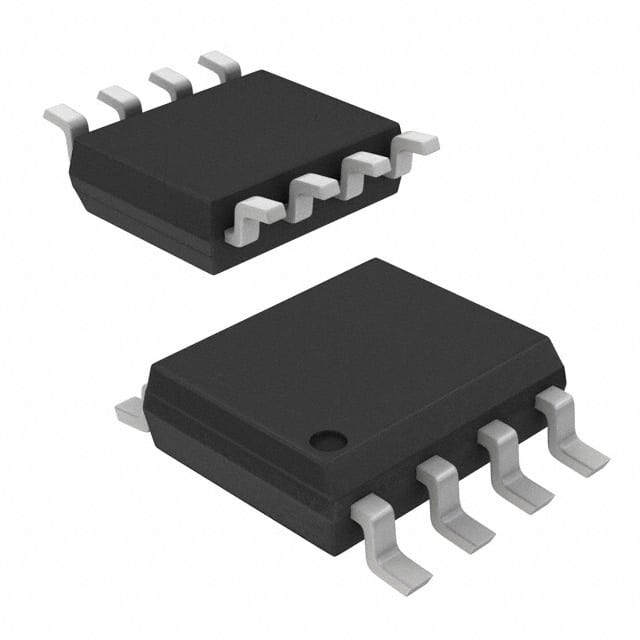
- Package: TO-252 (DPAK)
- Essence: Semiconductor component for power management
- Packaging/Quantity: Typically packaged in reels or tubes, quantity varies based on manufacturer
Specifications
- Voltage Rating: 30V
- Current Rating: 12A
- On-Resistance: 9.5mΩ
- Gate Charge: 15nC
- Operating Temperature Range: -55°C to 150°C
- Package Type: TO-252 (DPAK)
Detailed Pin Configuration
The FDS7082N3 typically has three pins: 1. Gate (G): Input pin for controlling the MOSFET 2. Drain (D): Output pin connected to the load 3. Source (S): Ground reference for the MOSFET
Functional Features
- High power handling capacity
- Low on-resistance leading to minimal power loss
- Fast switching speed for efficient operation
Advantages and Disadvantages
Advantages
- Efficient power management
- Suitable for high-frequency applications
- Compact package size
Disadvantages
- Sensitive to static electricity
- Requires careful handling during assembly
Working Principles
The FDS7082N3 operates based on the principle of field-effect transistors. When a voltage is applied to the gate terminal, it creates an electric field that controls the flow of current between the drain and source terminals. This enables the efficient switching and control of power within electronic circuits.
Detailed Application Field Plans
The FDS7082N3 finds extensive use in various applications including: - Switching power supplies - Motor control circuits - LED lighting systems - Battery management systems
Detailed and Complete Alternative Models
Some alternative models to the FDS7082N3 include: - IRF3708ZPbF - SI7850DP-T1-GE3 - AON6514
In conclusion, the FDS7082N3 is a versatile power MOSFET with excellent characteristics and functional features, making it suitable for a wide range of electronic applications.
(Word count: 398)
Liệt kê 10 câu hỏi và câu trả lời thường gặp liên quan đến ứng dụng FDS7082N3 trong giải pháp kỹ thuật
What is FDS7082N3?
- FDS7082N3 is a power MOSFET designed for various technical solutions, including power management and switching applications.
What are the key features of FDS7082N3?
- The key features of FDS7082N3 include low on-resistance, high current capability, and a compact package design for efficient power management.
What voltage and current ratings does FDS7082N3 support?
- FDS7082N3 supports voltage ratings up to [insert voltage rating] and current ratings up to [insert current rating], making it suitable for a wide range of applications.
In what types of technical solutions can FDS7082N3 be used?
- FDS7082N3 can be used in various technical solutions such as motor control, DC-DC converters, power supplies, and battery management systems.
What is the thermal performance of FDS7082N3?
- FDS7082N3 offers excellent thermal performance, with low thermal resistance and efficient heat dissipation capabilities.
Does FDS7082N3 have built-in protection features?
- Yes, FDS7082N3 is equipped with built-in protection features such as overcurrent protection and thermal shutdown to ensure reliable operation in demanding applications.
Is FDS7082N3 RoHS compliant?
- Yes, FDS7082N3 is RoHS compliant, meeting environmental standards for lead-free and hazardous substance-free manufacturing.
What are the recommended operating conditions for FDS7082N3?
- The recommended operating conditions for FDS7082N3 include a specified voltage range, temperature range, and current limits for optimal performance.
Can FDS7082N3 be used in automotive applications?
- Yes, FDS7082N3 is suitable for automotive applications, offering robust performance and reliability in harsh operating environments.
Where can I find detailed technical specifications and application notes for FDS7082N3?
- Detailed technical specifications and application notes for FDS7082N3 can be found in the product datasheet and application guides provided by the manufacturer.