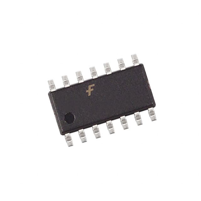
Xem thông số kỹ thuật để biết chi tiết sản phẩm.

74LVX04SJ
Basic Information Overview
- Category: Integrated Circuit (IC)
- Use: Inverter
- Characteristics: High-speed, low-power, hex inverter
- Package: SOIC (Small Outline Integrated Circuit)
- Essence: Logic gate
- Packaging/Quantity: Tape and reel, 2500 pieces per reel
Specifications
- Supply Voltage Range: 2.0V to 5.5V
- Input Voltage Range: 0V to VCC
- Output Voltage Range: 0V to VCC
- Maximum Input Current: ±1mA
- Maximum Output Current: ±8mA
- Propagation Delay Time: 6ns (typical)
Detailed Pin Configuration
The 74LVX04SJ has a total of 14 pins. The pin configuration is as follows:
Pin 1: Input A1
Pin 2: Output Y1
Pin 3: Input A2
Pin 4: Output Y2
Pin 5: Ground (GND)
Pin 6: Input A3
Pin 7: Output Y3
Pin 8: VCC
Pin 9: Output Y4
Pin 10: Input A4
Pin 11: Output Y5
Pin 12: Input A5
Pin 13: Output Y6
Pin 14: Input A6
Functional Features
- Hex inverter with high-speed operation
- Low power consumption
- Wide supply voltage range for compatibility with various systems
- TTL (Transistor-Transistor Logic) compatible inputs
- CMOS (Complementary Metal-Oxide-Semiconductor) output levels
Advantages and Disadvantages
Advantages: - Fast switching speed - Low power consumption - Wide operating voltage range - Compatibility with TTL inputs
Disadvantages: - Limited output current capability - Not suitable for high-power applications
Working Principles
The 74LVX04SJ is a hex inverter IC that converts input logic levels to their complementary values. It operates by using a combination of transistors and resistors to invert the input signal. The output is the logical complement of the input, i.e., when the input is high, the output is low, and vice versa.
Detailed Application Field Plans
The 74LVX04SJ can be used in various digital systems and applications, including: 1. Microcontrollers and microprocessors 2. Communication systems 3. Data transmission equipment 4. Industrial automation 5. Consumer electronics 6. Automotive electronics
Detailed and Complete Alternative Models
Some alternative models that can be used as substitutes for the 74LVX04SJ are: - SN74LVC04A - MC74LVX04 - CD74HCT04E - TC7SZ04FU
These alternatives offer similar functionality and characteristics, allowing users to choose the most suitable option for their specific requirements.
In conclusion, the 74LVX04SJ is a high-speed, low-power hex inverter IC that finds applications in various digital systems. Its advantages include fast switching speed, low power consumption, and wide operating voltage range. However, it has limited output current capability and may not be suitable for high-power applications. Users can consider alternative models such as SN74LVC04A or MC74LVX04 as substitutes.
Liệt kê 10 câu hỏi và câu trả lời thường gặp liên quan đến ứng dụng 74LVX04SJ trong giải pháp kỹ thuật
Sure! Here are 10 common questions and answers related to the application of 74LVX04SJ in technical solutions:
Q: What is the 74LVX04SJ? A: The 74LVX04SJ is a hex inverter gate IC, which means it has six individual inverters on a single chip.
Q: What is the voltage supply range for the 74LVX04SJ? A: The 74LVX04SJ operates with a voltage supply range of 2V to 5.5V.
Q: What is the maximum output current of the 74LVX04SJ? A: The maximum output current of the 74LVX04SJ is typically around 8mA.
Q: Can the 74LVX04SJ be used as a level shifter? A: Yes, the 74LVX04SJ can be used as a level shifter to convert signals between different voltage levels.
Q: How many inputs and outputs does each inverter have? A: Each inverter in the 74LVX04SJ has one input and one output.
Q: What is the propagation delay of the 74LVX04SJ? A: The propagation delay of the 74LVX04SJ is typically around 7ns.
Q: Can the 74LVX04SJ be used in high-speed applications? A: Yes, the 74LVX04SJ is designed for high-speed operation and can be used in various high-frequency applications.
Q: Is the 74LVX04SJ compatible with TTL logic levels? A: Yes, the 74LVX04SJ is compatible with both TTL and CMOS logic levels.
Q: Can the 74LVX04SJ be used in battery-powered applications? A: Yes, the 74LVX04SJ has a low power consumption and can be used in battery-powered applications.
Q: What is the package type of the 74LVX04SJ? A: The 74LVX04SJ is available in a small outline (SO) package, specifically SOIC-14.
Please note that these answers are general and may vary depending on specific datasheet specifications or application requirements.

