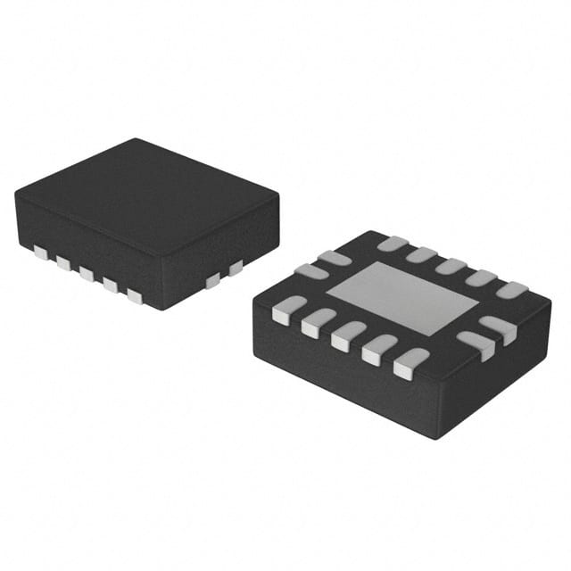
Xem thông số kỹ thuật để biết chi tiết sản phẩm.

Encyclopedia Entry: 74HCT08BQ-Q100,115
Product Overview
Category
The 74HCT08BQ-Q100,115 belongs to the category of integrated circuits (ICs) and specifically falls under the logic gates subcategory.
Use
This product is commonly used in digital electronics for logical operations. It serves as a quad 2-input AND gate, allowing for the implementation of various logical functions.
Characteristics
- High-speed operation
- Wide supply voltage range
- Low power consumption
- Schmitt-trigger inputs for noise immunity
- Balanced propagation delays
- Symmetrical output impedance
Package
The 74HCT08BQ-Q100,115 is available in a small outline package (SOT353), which is a surface-mount package with four pins.
Essence
The essence of this product lies in its ability to perform logical AND operations on two input signals, providing an output signal based on their logical combination.
Packaging/Quantity
The 74HCT08BQ-Q100,115 is typically packaged in reels or tape and reel format, containing a specific quantity of units per reel.
Specifications
- Supply Voltage Range: 2 V to 6 V
- Input Voltage Range: 0 V to VCC
- Output Voltage Range: 0 V to VCC
- Operating Temperature Range: -40°C to +125°C
- Input Capacitance: 3.5 pF
- Output Capacitance: 4.5 pF
- Propagation Delay: 10 ns (max)
- Quiescent Current: 1 µA (typ)
Detailed Pin Configuration
The 74HCT08BQ-Q100,115 has four pins arranged as follows:
____
   A1 -|    |- VCC
   B1 -|    |- Y1
   A2 -|    |- B2
   GND -|____|- Y2
Functional Features
- Quad 2-input AND gate: The 74HCT08BQ-Q100,115 can perform logical AND operations on two input signals, providing a corresponding output signal.
- Schmitt-trigger inputs: These inputs ensure noise immunity by providing hysteresis and reducing the impact of signal fluctuations.
- Balanced propagation delays: The product maintains balanced delays across all inputs, ensuring accurate timing in logical operations.
- Wide supply voltage range: It can operate within a wide range of supply voltages, making it versatile for various applications.
Advantages and Disadvantages
Advantages
- High-speed operation allows for efficient processing of logical operations.
- Low power consumption makes it suitable for battery-powered devices.
- Schmitt-trigger inputs provide noise immunity, enhancing reliability.
- Wide supply voltage range enables compatibility with different systems.
Disadvantages
- Limited to performing only AND operations, requiring additional logic gates for other logical functions.
- Surface-mount package may require specialized equipment for soldering and replacement.
Working Principles
The 74HCT08BQ-Q100,115 operates based on the principles of digital logic. When both input signals are high (logic level 1), the output signal is also high. If any of the input signals are low (logic level 0), the output signal becomes low. This behavior follows the truth table of an AND gate.
Detailed Application Field Plans
The 74HCT08BQ-Q100,115 finds application in various fields, including: 1. Digital circuit design: It is commonly used in the design of digital systems, such as microcontrollers, CPUs, and memory units. 2. Communication systems: The product can be utilized in communication systems for signal processing and logical operations. 3. Industrial automation: It plays a crucial role in controlling and processing signals in industrial automation systems. 4. Consumer electronics: The 74HCT08BQ-Q100,115 is found in devices like smartphones, tablets, and gaming consoles for logical operations.
Detailed and Complete Alternative Models
Some alternative models to the 74HCT08BQ-Q100,115 include: - 74LS08: A TTL (Transistor-Transistor Logic) version of the quad 2-input AND gate. - CD4081: A CMOS (Complementary Metal-Oxide-Semiconductor) quad 2-input AND gate. - SN54LS08: Another TTL variant with similar functionality.
These alternative models offer similar logical functions but may differ in terms of power consumption, speed, and voltage compatibility.
In conclusion, the 74HCT08BQ-Q100,115 is a versatile integrated circuit that serves as a quad 2-input AND gate. Its high-speed operation, low power consumption, and noise immunity make it suitable for various digital applications. While limited to AND operations, it can be combined with other logic gates to achieve more complex functions
Liệt kê 10 câu hỏi và câu trả lời thường gặp liên quan đến ứng dụng 74HCT08BQ-Q100,115 trong giải pháp kỹ thuật
Sure! Here are 10 common questions and answers related to the application of 74HCT08BQ-Q100,115 in technical solutions:
Question: What is the function of the 74HCT08BQ-Q100,115?
Answer: The 74HCT08BQ-Q100,115 is a quad 2-input AND gate that performs logical AND operations on two input signals.Question: What is the operating voltage range for this IC?
Answer: The 74HCT08BQ-Q100,115 operates within a voltage range of 4.5V to 5.5V.Question: Can I use this IC with a higher voltage supply?
Answer: No, exceeding the specified voltage range can damage the IC. It is recommended to stay within the specified voltage range.Question: What is the maximum current that can be sourced or sunk by each output pin?
Answer: Each output pin of the 74HCT08BQ-Q100,115 can source or sink up to 4mA of current.Question: Can I connect multiple inputs together to create a multi-input AND gate?
Answer: Yes, you can connect multiple inputs together to create a multi-input AND gate using the 74HCT08BQ-Q100,115.Question: What is the propagation delay of this IC?
Answer: The propagation delay of the 74HCT08BQ-Q100,115 is typically around 9ns.Question: Can I use this IC in high-speed applications?
Answer: Yes, the 74HCT08BQ-Q100,115 is suitable for high-speed applications due to its low propagation delay.Question: Is this IC compatible with both TTL and CMOS logic levels?
Answer: Yes, the 74HCT08BQ-Q100,115 is compatible with both TTL and CMOS logic levels.Question: Can I use this IC in automotive applications?
Answer: Yes, the 74HCT08BQ-Q100,115 is specifically designed for automotive applications and meets the required standards.Question: Are there any recommended decoupling capacitors for this IC?
Answer: It is recommended to place a 0.1μF ceramic capacitor between VCC and GND pins of the IC for proper decoupling.
Please note that these answers are general and may vary depending on the specific application and requirements.

