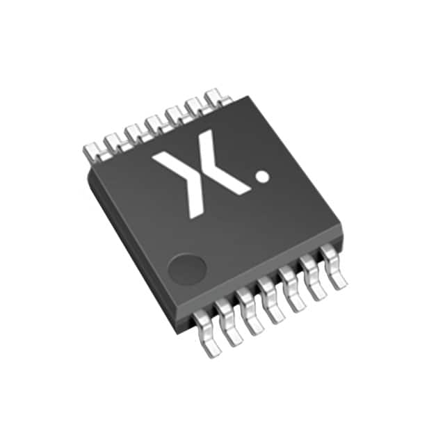
Xem thông số kỹ thuật để biết chi tiết sản phẩm.

Encyclopedia Entry: 74ALVC04PW,118
Product Overview
Category
The 74ALVC04PW,118 belongs to the category of integrated circuits (ICs) and specifically falls under the family of logic gates.
Use
This product is commonly used in digital electronics for signal processing and logical operations. It serves as an inverter gate, converting input signals into their complementary outputs.
Characteristics
- Low voltage operation: The 74ALVC04PW,118 operates at a low voltage range, typically between 1.65V and 3.6V.
- High-speed performance: It offers fast propagation delay times, making it suitable for high-frequency applications.
- Wide temperature range: This IC can operate reliably across a wide temperature range, from -40°C to 125°C.
- Low power consumption: The 74ALVC04PW,118 consumes minimal power, making it energy-efficient.
Package and Quantity
The 74ALVC04PW,118 is available in a small-sized package known as TSSOP-14. It is supplied in tape and reel packaging, with a quantity of 2500 units per reel.
Specifications
- Supply Voltage Range: 1.65V to 3.6V
- Input Voltage Range: 0V to VCC
- Output Voltage Range: 0V to VCC
- Maximum Operating Frequency: 200 MHz
- Propagation Delay Time: 2.5 ns (typical)
- Input Capacitance: 3 pF (typical)
- Output Current: ±24 mA
Pin Configuration
The 74ALVC04PW,118 has a total of 14 pins arranged as follows:
+---+--+---+
   A1 -|1  +--+ 14|- VCC
   A2 -|2        13|- Y1
   A3 -|3        12|- Y2
   A4 -|4        11|- Y3
   A5 -|5   74ALVC04PW,118   10|- Y4
   A6 -|6        9 |- Y5
   A7 -|7        8 |- GND
       +----------+
Functional Features
The 74ALVC04PW,118 is a hex inverter gate that performs logical inversion on its input signals. It has six independent inverters, each capable of converting a high-level input signal to a low-level output and vice versa.
Advantages and Disadvantages
Advantages
- Low voltage operation enables compatibility with modern low-power devices.
- High-speed performance allows for efficient signal processing in time-critical applications.
- Wide temperature range ensures reliable operation in various environmental conditions.
- Small package size saves board space and facilitates compact designs.
Disadvantages
- Limited output current may restrict its use in certain high-current applications.
- Lack of built-in protection features may require additional circuitry for robustness.
Working Principles
The 74ALVC04PW,118 operates based on the principles of complementary metal-oxide-semiconductor (CMOS) technology. It utilizes a combination of p-type and n-type MOSFETs to achieve logical inversion. When the input voltage is high, the output is driven low, and vice versa.
Application Field Plans
The 74ALVC04PW,118 finds extensive application in various digital systems, including but not limited to: - Microprocessors and microcontrollers - Communication systems - Data storage devices - Consumer electronics - Automotive electronics
Its ability to perform logical inversion makes it suitable for tasks such as signal conditioning, level shifting, clock synchronization, and data manipulation.
Alternative Models
There are several alternative models available in the market that offer similar functionality to the 74ALVC04PW,118. Some notable alternatives include: - SN74LVC04A - MC74VHC1G04 - CD4049UB
These alternatives may vary in terms of voltage range, speed, package type, and other specifications. It is important to consider specific requirements and compatibility when selecting an alternative model.
In conclusion, the 74ALVC04PW,118 is a versatile hex inverter gate IC that operates at low voltage, offers high-speed performance, and finds application in various digital systems. Its compact size, wide temperature range, and energy efficiency make it a popular choice among designers seeking reliable logic inversion capabilities.
Word Count: 530
Liệt kê 10 câu hỏi và câu trả lời thường gặp liên quan đến ứng dụng 74ALVC04PW,118 trong giải pháp kỹ thuật
Sure! Here are 10 common questions and answers related to the application of 74ALVC04PW,118:
Q: What is the 74ALVC04PW,118? A: The 74ALVC04PW,118 is a hex inverter IC (Integrated Circuit) that consists of six independent inverters.
Q: What is the operating voltage range for the 74ALVC04PW,118? A: The operating voltage range for this IC is typically between 1.65V and 3.6V.
Q: What is the maximum output current of the 74ALVC04PW,118? A: The maximum output current per channel is around 24mA.
Q: Can I use the 74ALVC04PW,118 with a 5V power supply? A: No, this IC is not designed to be used with a 5V power supply. It is specifically designed for lower voltage applications.
Q: What is the typical propagation delay of the 74ALVC04PW,118? A: The typical propagation delay for this IC is around 3.7ns.
Q: Can I connect the inputs of the 74ALVC04PW,118 directly to a microcontroller or FPGA? A: Yes, the inputs are compatible with standard CMOS logic levels, so they can be connected directly to microcontrollers or FPGAs.
Q: Is the 74ALVC04PW,118 suitable for high-speed applications? A: Yes, this IC is designed for high-speed operation and can be used in various high-frequency applications.
Q: Does the 74ALVC04PW,118 have built-in protection features? A: No, this IC does not have built-in protection features. External protection measures may be required depending on the application.
Q: Can I use the 74ALVC04PW,118 in both digital and analog circuits? A: Yes, this IC can be used in both digital and analog circuits, but it is primarily designed for digital logic applications.
Q: What package options are available for the 74ALVC04PW,118? A: The 74ALVC04PW,118 is available in various package options, such as TSSOP, VSSOP, and DHVQFN, to suit different PCB layout requirements.
Please note that these answers are general and may vary depending on the specific datasheet and manufacturer's specifications for the 74ALVC04PW,118.

