

Xem thông số kỹ thuật để biết chi tiết sản phẩm.
Encyclopedia Entry: 74AHCT2G08DC-Q100H
Product Overview
Category
The 74AHCT2G08DC-Q100H belongs to the category of integrated circuits (ICs).
Use
This IC is commonly used in digital logic applications for performing logical AND operations.
Characteristics
- High-speed operation
- Low power consumption
- Wide operating voltage range
- Schmitt-trigger inputs for noise immunity
- Compatible with TTL and CMOS logic families
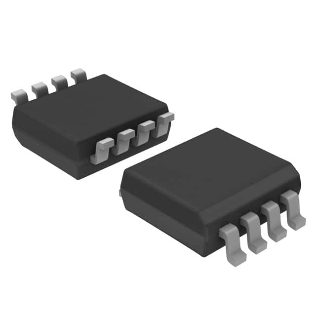
Package
The 74AHCT2G08DC-Q100H is available in a small outline package (SOT) with two gates per package.
Essence
The essence of this product lies in its ability to provide reliable and efficient logical AND operations in various electronic devices.
Packaging/Quantity
The 74AHCT2G08DC-Q100H is typically packaged in reels or tubes, containing a specific quantity of ICs per package. The exact packaging and quantity may vary depending on the manufacturer.
Specifications
- Supply Voltage Range: 4.5V to 5.5V
- Input Voltage Range: 0V to VCC
- Output Voltage Range: 0V to VCC
- Operating Temperature Range: -40°C to +125°C
- Logic Family: AHCT
- Number of Gates: 2
Detailed Pin Configuration
The 74AHCT2G08DC-Q100H has a total of 8 pins, which are assigned specific functions as follows:
- A Input 1
- B Input 1
- Y Output 1
- GND (Ground)
- Y Output 2
- B Input 2
- A Input 2
- VCC (Supply Voltage)
Functional Features
- Logical AND operation: The 74AHCT2G08DC-Q100H performs the logical AND operation on two input signals (A and B) and provides the corresponding output signal (Y).
- Schmitt-trigger inputs: The IC incorporates Schmitt-trigger inputs, which enhance noise immunity by providing hysteresis.
- Wide operating voltage range: The IC can operate within a wide voltage range, making it suitable for various applications.
- Compatibility with TTL and CMOS logic families: The 74AHCT2G08DC-Q100H is compatible with both transistor-transistor logic (TTL) and complementary metal-oxide-semiconductor (CMOS) logic families.
Advantages and Disadvantages
Advantages
- High-speed operation allows for efficient processing of logical AND operations.
- Low power consumption makes it suitable for battery-powered devices.
- Schmitt-trigger inputs provide improved noise immunity.
- Wide operating voltage range enables versatile application possibilities.
- Compatibility with TTL and CMOS logic families ensures easy integration into existing systems.
Disadvantages
- Limited number of gates per package may require multiple ICs for complex logic circuits.
- Sensitive to electrostatic discharge (ESD), requiring proper handling during installation and usage.
Working Principles
The 74AHCT2G08DC-Q100H operates based on the principles of digital logic. It utilizes transistors and other electronic components to perform logical AND operations on the input signals. The internal circuitry processes the input signals and generates the corresponding output signal based on the logical AND function.
Detailed Application Field Plans
The 74AHCT2G08DC-Q100H finds applications in various fields, including but not limited to: 1. Digital electronics 2. Microcontrollers 3. Communication systems 4. Automotive electronics 5. Industrial automation
Detailed and Complete Alternative Models
Some alternative models that offer similar functionality to the 74AHCT2G08DC-Q100H include: - 74HC08: This IC is compatible with CMOS logic and offers similar characteristics and pin configuration. - SN74LS08: A TTL-compatible IC that performs logical AND operations with comparable specifications.
These alternative models can be considered based on specific requirements and compatibility with existing systems.
Word count: 554 words
Liệt kê 10 câu hỏi và câu trả lời thường gặp liên quan đến ứng dụng 74AHCT2G08DC-Q100H trong giải pháp kỹ thuật
Sure! Here are 10 common questions and answers related to the application of 74AHCT2G08DC-Q100H in technical solutions:
Q: What is the 74AHCT2G08DC-Q100H? A: The 74AHCT2G08DC-Q100H is a dual 2-input AND gate integrated circuit (IC) that operates at high-speed and low power consumption.
Q: What is the voltage supply range for this IC? A: The 74AHCT2G08DC-Q100H has a voltage supply range of 4.5V to 5.5V.
Q: What is the maximum operating frequency of this IC? A: The maximum operating frequency of the 74AHCT2G08DC-Q100H is typically around 125 MHz.
Q: Can this IC be used in automotive applications? A: Yes, the 74AHCT2G08DC-Q100H is specifically designed for automotive applications and meets the AEC-Q100 automotive qualification standards.
Q: What is the output drive capability of this IC? A: The 74AHCT2G08DC-Q100H has a typical output drive capability of 8 mA.
Q: Is this IC compatible with both CMOS and TTL logic levels? A: Yes, the 74AHCT2G08DC-Q100H is compatible with both CMOS and TTL logic levels, making it versatile for various applications.
Q: Does this IC have built-in protection features? A: Yes, the 74AHCT2G08DC-Q100H has built-in ESD protection on all inputs and outputs, ensuring robustness against electrostatic discharge.
Q: Can this IC be used in battery-powered applications? A: Yes, the 74AHCT2G08DC-Q100H is suitable for battery-powered applications due to its low power consumption.
Q: What is the operating temperature range of this IC? A: The 74AHCT2G08DC-Q100H has an operating temperature range of -40°C to +125°C, making it suitable for a wide range of environments.
Q: Are there any recommended application circuits available for this IC? A: Yes, the datasheet of the 74AHCT2G08DC-Q100H provides recommended application circuits and example schematics to help with implementation.
Please note that these answers are general and may vary depending on the specific datasheet and manufacturer's specifications for the 74AHCT2G08DC-Q100H.