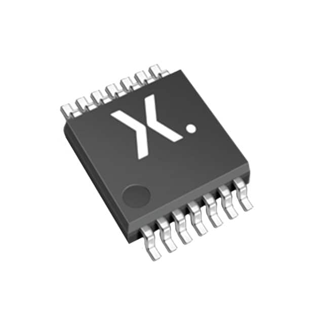
Xem thông số kỹ thuật để biết chi tiết sản phẩm.

74AHC30PW-Q100J
Product Overview
Category
The 74AHC30PW-Q100J belongs to the category of integrated circuits (ICs).
Use
This IC is commonly used in digital logic applications.
Characteristics
- High-speed operation
- Low power consumption
- Wide operating voltage range
- Compatibility with TTL levels
- Schmitt-trigger action on all inputs
- Balanced propagation delays
- Direct interface with CMOS, NMOS, and TTL circuits
Package
The 74AHC30PW-Q100J is available in a small-sized TSSOP package.
Essence
This IC is an advanced high-speed CMOS device that provides reliable digital logic functionality.
Packaging/Quantity
The 74AHC30PW-Q100J is typically packaged in reels or tubes, with a quantity of 2500 units per reel/tube.
Specifications
- Supply voltage: 2 V to 5.5 V
- Input voltage: -0.5 V to VCC + 0.5 V
- Output voltage: 0 V to VCC
- Operating temperature range: -40°C to +125°C
- Maximum input current: ±20 mA
- Maximum output current: ±25 mA
- Propagation delay: 6 ns (typical)
Detailed Pin Configuration
The 74AHC30PW-Q100J has a total of 14 pins, numbered as follows:
- A1
- B1
- Y1
- A2
- B2
- Y2
- GND
- C1
- D1
- Y3
- C2
- D2
- Y4
- VCC
Functional Features
- The 74AHC30PW-Q100J is a quad 2-input NAND gate, which means it contains four separate NAND gates.
- Each NAND gate has two inputs (A and B) and one output (Y).
- The Schmitt-trigger action on all inputs allows the IC to have hysteresis, making it less susceptible to noise and providing better noise immunity.
- The balanced propagation delays ensure that all outputs switch simultaneously when inputs change.
Advantages and Disadvantages
Advantages
- High-speed operation enables efficient digital logic processing.
- Low power consumption makes it suitable for battery-powered devices.
- Wide operating voltage range allows compatibility with various systems.
- Schmitt-trigger action provides improved noise immunity.
- Direct interface with CMOS, NMOS, and TTL circuits simplifies integration.
Disadvantages
- Limited number of NAND gates in a single IC package.
- Not suitable for applications requiring a large number of logic gates.
Working Principles
The 74AHC30PW-Q100J operates based on the principles of digital logic. When both inputs of a NAND gate are high (logic level 1), the output is low (logic level 0). In all other cases, the output is high. This behavior allows the IC to perform logical operations such as AND, OR, and NOT.
Detailed Application Field Plans
The 74AHC30PW-Q100J finds applications in various fields, including: - Digital signal processing - Microcontroller-based systems - Communication systems - Industrial automation - Consumer electronics
Detailed and Complete Alternative Models
Some alternative models to the 74AHC30PW-Q100J include: - SN74AHC30-Q1 - CD74AHC30-Q1 - MC74AHC30-Q1 - TC74AHC30-Q1
These models offer similar functionality and characteristics, providing alternatives for different sourcing or specific requirements.
Word count: 511 words
Liệt kê 10 câu hỏi và câu trả lời thường gặp liên quan đến ứng dụng 74AHC30PW-Q100J trong giải pháp kỹ thuật
Sure! Here are 10 common questions and answers related to the application of 74AHC30PW-Q100J in technical solutions:
1. What is the 74AHC30PW-Q100J? - The 74AHC30PW-Q100J is a 8-input NAND gate IC (integrated circuit) that operates on a wide voltage range and is designed for automotive applications.
2. What is the operating voltage range of the 74AHC30PW-Q100J? - The operating voltage range of the 74AHC30PW-Q100J is from 2 V to 5.5 V.
3. How many inputs does the 74AHC30PW-Q100J have? - The 74AHC30PW-Q100J has 8 inputs, allowing it to perform logical operations on multiple signals simultaneously.
4. What is the maximum output current of the 74AHC30PW-Q100J? - The maximum output current of the 74AHC30PW-Q100J is 8 mA.
5. Can the 74AHC30PW-Q100J be used in automotive applications? - Yes, the 74AHC30PW-Q100J is specifically designed for automotive applications and meets the necessary quality and reliability standards.
6. What is the propagation delay of the 74AHC30PW-Q100J? - The propagation delay of the 74AHC30PW-Q100J is typically around 7 ns.
7. Is the 74AHC30PW-Q100J compatible with other logic families? - Yes, the 74AHC30PW-Q100J is compatible with both CMOS and TTL logic families.
8. Can the 74AHC30PW-Q100J be used in high-speed applications? - Yes, the 74AHC30PW-Q100J is suitable for high-speed applications due to its low propagation delay and compatibility with various logic families.
9. What is the package type of the 74AHC30PW-Q100J? - The 74AHC30PW-Q100J comes in a TSSOP (Thin Shrink Small Outline Package) package.
10. Are there any special considerations when using the 74AHC30PW-Q100J? - It is important to ensure that the power supply voltage does not exceed the specified range, and proper decoupling capacitors should be used to minimize noise and voltage fluctuations.
Please note that these answers are general and may vary depending on the specific application and requirements.

