

Xem thông số kỹ thuật để biết chi tiết sản phẩm.
MS105/TR12 Product Overview
Introduction
MS105/TR12 is a component belonging to the category of integrated circuits. It is widely used in electronic devices for various applications due to its unique characteristics and functional features. This entry provides an overview of the product, including its specifications, pin configuration, advantages, disadvantages, working principles, application field plans, and alternative models.
Basic Information Overview
- Category: Integrated Circuits
- Use: Electronic Devices
- Characteristics: High performance, reliability, compact size
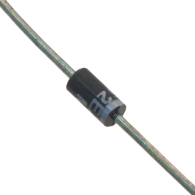
- Package: DIP (Dual Inline Package)
- Essence: Microcontroller unit
- Packaging/Quantity: Typically packaged in tubes or trays, quantity varies based on manufacturer
Specifications
- Operating Voltage: 3.3V - 5V
- Clock Speed: Up to 16 MHz
- I/O Pins: 12
- Memory: 1KB Flash, 32B SRAM
- Communication Interfaces: SPI, I2C, UART
Detailed Pin Configuration
The detailed pin configuration of MS105/TR12 is as follows: 1. VCC 2. GND 3. Reset 4. Digital I/O 0 (DIO0) 5. Digital I/O 1 (DIO1) 6. Analog Input 0 (AIO0) 7. Analog Input 1 (AIO1) 8. Serial Clock (SCK) 9. Serial Data Input/Output (SDIO) 10. Chip Select (CS) 11. UART Transmit (TX) 12. UART Receive (RX)
Functional Features
- Microcontroller with embedded memory and communication interfaces
- Low power consumption
- Compact form factor
- Easy integration with other electronic components
Advantages and Disadvantages
Advantages
- Versatile for various electronic applications
- Low power consumption
- Small footprint
- Integrated memory and communication interfaces
Disadvantages
- Limited memory capacity
- Restricted number of I/O pins
Working Principles
MS105/TR12 operates as a microcontroller unit, executing instructions stored in its flash memory. It interacts with external devices through its I/O pins and communication interfaces, enabling control and data exchange within electronic systems.
Detailed Application Field Plans
MS105/TR12 finds extensive use in the following application fields: - Home automation systems - Sensor nodes - Wearable devices - IoT (Internet of Things) devices - Embedded control systems
Detailed and Complete Alternative Models
Some alternative models to MS105/TR12 include: - ATmega328P - PIC16F877A - STM32F103C8T6 - ESP8266
In conclusion, MS105/TR12 is a versatile integrated circuit suitable for a wide range of electronic applications, offering a balance of performance, size, and functionality.
Word Count: 411
Liệt kê 10 câu hỏi và câu trả lời thường gặp liên quan đến ứng dụng MS105/TR12 trong giải pháp kỹ thuật
What is MS105/TR12?
- MS105/TR12 refers to a specific technical standard or requirement for a particular application.
How does MS105/TR12 impact technical solutions?
- MS105/TR12 sets the guidelines and specifications that technical solutions must adhere to in order to meet the required standards.
What are the key components of MS105/TR12?
- The key components of MS105/TR12 may include performance criteria, material specifications, testing methods, and compliance requirements.
Is compliance with MS105/TR12 mandatory?
- Compliance with MS105/TR12 may be mandatory depending on the industry regulations or customer requirements.
How can I ensure my technical solution meets MS105/TR12 standards?
- To ensure compliance, it's important to thoroughly understand the requirements outlined in MS105/TR12 and incorporate them into the design and development process.
Are there any common challenges in implementing MS105/TR12 in technical solutions?
- Common challenges may include sourcing compliant materials, meeting performance criteria, and ensuring consistent quality control.
Can deviations from MS105/TR12 be allowed under certain circumstances?
- Deviations from MS105/TR12 may be allowed if they are justified and do not compromise the overall safety or performance of the technical solution.
What are the potential consequences of non-compliance with MS105/TR12?
- Non-compliance could lead to rejection of the technical solution, legal implications, or damage to the reputation of the organization.
Are there any resources available to help understand and implement MS105/TR12?
- Industry associations, technical forums, and official documentation related to MS105/TR12 can provide valuable guidance.
How often does MS105/TR12 get updated, and how can I stay informed about changes?
- Updates to MS105/TR12 may occur periodically, and staying informed can be achieved through subscribing to relevant industry publications or monitoring official channels for announcements.