

Xem thông số kỹ thuật để biết chi tiết sản phẩm.
24LC256-I/MF
Product Overview
Category
The 24LC256-I/MF belongs to the category of electrically erasable programmable read-only memory (EEPROM) chips.
Use
This chip is commonly used for non-volatile data storage in various electronic devices, such as microcontrollers, computers, and consumer electronics.
Characteristics
- Non-volatile: The 24LC256-I/MF retains stored data even when power is removed.
- High capacity: It has a storage capacity of 256 kilobits (32 kilobytes).
- Low power consumption: This chip operates at low power levels, making it suitable for battery-powered devices.
- I2C interface: It communicates using the Inter-Integrated Circuit (I2C) protocol, allowing for easy integration into existing systems.
Package
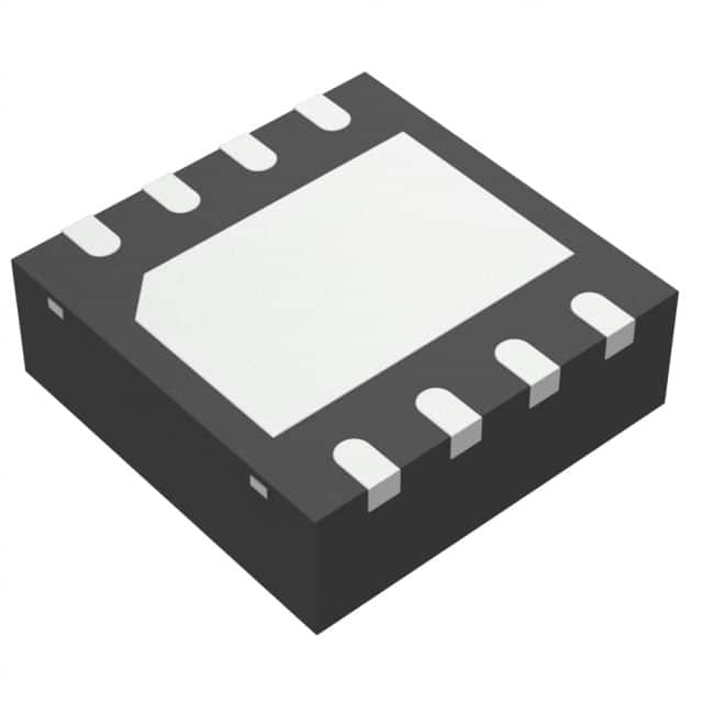
The 24LC256-I/MF is available in an 8-pin SOIC (Small Outline Integrated Circuit) package. This package offers compactness and ease of soldering.
Essence
The essence of the 24LC256-I/MF lies in its ability to provide reliable and non-volatile data storage in a compact form factor.
Packaging/Quantity
This chip is typically sold in reels or tubes, with each reel or tube containing a specific quantity of chips. The exact packaging and quantity may vary depending on the supplier.
Specifications
- Storage Capacity: 256 kilobits (32 kilobytes)
- Interface: I2C
- Operating Voltage: 1.7V to 5.5V
- Operating Temperature Range: -40°C to +85°C
- Write Endurance: 1,000,000 cycles
- Data Retention: 200 years
Detailed Pin Configuration
The 24LC256-I/MF has eight pins, which are assigned specific functions:
- VCC: Power supply voltage input
- SDA: Serial data input/output for I2C communication
- SCL: Serial clock input for I2C communication
- WP: Write protect pin (optional)
- VSS: Ground reference
- NC: No connection (unused pin)
- NC: No connection (unused pin)
- VCC: Power supply voltage input
Functional Features
- Byte-level Read/Write: The 24LC256-I/MF allows individual bytes to be read from or written to the memory array.
- Sequential Read: It supports sequential reading of multiple bytes, enabling efficient data retrieval.
- Hardware Write Protection: The WP pin can be used to protect the memory contents from accidental writes.
- Self-Timed Programming Cycle: The chip automatically manages the programming cycle, simplifying the write operation.
Advantages and Disadvantages
Advantages
- Non-volatile storage: Data is retained even without power.
- High capacity: Ample storage space for various applications.
- Low power consumption: Suitable for battery-powered devices.
- Compact form factor: Easy integration into electronic systems.
- I2C interface: Simple and widely supported communication protocol.
Disadvantages
- Limited write endurance: The chip has a finite number of write cycles.
- Relatively slower write speed compared to other memory technologies.
- Vulnerable to electromagnetic interference (EMI) due to its non-shielded package.
Working Principles
The 24LC256-I/MF utilizes EEPROM technology to store data. It consists of an array of floating-gate transistors that can be electrically programmed and erased. When data is written, charges are trapped in the floating gates, altering the transistor's behavior and storing the information. Reading the stored data involves sensing the transistor's state and converting it back into digital information.
Detailed Application Field Plans
The 24LC256-I/MF finds applications in various fields, including:
- Embedded Systems: Used for storing configuration data, firmware updates, and user settings in microcontroller-based systems.
- Consumer Electronics: Employed in devices like smart TVs, set-top boxes, and audio equipment to store user preferences and system parameters.
- Automotive: Utilized for storing critical data, such as calibration values and fault codes, in automotive electronic control units (ECUs).
- Industrial Automation: Integrated into programmable logic controllers (PLCs) and industrial sensors for storing calibration data and device configurations.
Detailed and Complete Alternative Models
- 24LC512: A higher-capacity variant with 512 kilobits (64 kilobytes) of storage.
- 24LC128: A lower-capacity variant with 128 kilobits (16 kilobytes) of storage.
- 24LC01B: A lower-capacity variant with 1 kilobit (128 bytes) of storage.
These alternative models offer different storage capacities to suit specific application requirements.
In conclusion, the 24LC256-I/MF is a
Liệt kê 10 câu hỏi và câu trả lời thường gặp liên quan đến ứng dụng 24LC256-I/MF trong giải pháp kỹ thuật
What is the maximum clock frequency for 24LC256-I/MF?
- The maximum clock frequency for 24LC256-I/MF is 400 kHz.What is the operating voltage range for 24LC256-I/MF?
- The operating voltage range for 24LC256-I/MF is 1.7V to 5.5V.Can 24LC256-I/MF be used in automotive applications?
- Yes, 24LC256-I/MF is suitable for automotive applications.What is the typical write cycle time for 24LC256-I/MF?
- The typical write cycle time for 24LC256-I/MF is 5 ms.Is 24LC256-I/MF compatible with I2C protocol?
- Yes, 24LC256-I/MF is compatible with I2C protocol.What is the maximum data transfer rate for 24LC256-I/MF?
- The maximum data transfer rate for 24LC256-I/MF is 1000 kbps.Can 24LC256-I/MF operate in extended temperature ranges?
- Yes, 24LC256-I/MF can operate in extended temperature ranges from -40°C to 125°C.Does 24LC256-I/MF have built-in write protection?
- Yes, 24LC256-I/MF features built-in hardware write protection.What is the typical standby current for 24LC256-I/MF?
- The typical standby current for 24LC256-I/MF is 1 µA.Is 24LC256-I/MF RoHS compliant?
- Yes, 24LC256-I/MF is RoHS compliant.