

Xem thông số kỹ thuật để biết chi tiết sản phẩm.
MAX934CSE+ - Product Encyclopedia Entry
Introduction
The MAX934CSE+ is a versatile integrated circuit that belongs to the category of precision operational amplifiers. This entry provides an overview of the basic information, specifications, detailed pin configuration, functional features, advantages and disadvantages, working principles, detailed application field plans, and alternative models of the MAX934CSE+.
Basic Information Overview
- Category: Precision Operational Amplifiers
- Use: The MAX934CSE+ is commonly used in applications requiring high precision and low noise amplification, such as instrumentation, sensor signal conditioning, and data acquisition systems.
- Characteristics: It is known for its low offset voltage, low input bias current, and low noise, making it suitable for precision signal processing.
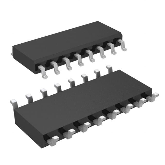
- Package: The MAX934CSE+ is available in a 16-pin narrow SO package.
- Essence: Its essence lies in providing accurate and stable amplification of input signals with minimal distortion.
- Packaging/Quantity: The MAX934CSE+ is typically available in tape and reel packaging with varying quantities based on the supplier.
Specifications
- Supply Voltage: ±2.25V to ±18V
- Input Offset Voltage: 50μV (max)
- Input Bias Current: 0.6pA (max)
- Gain Bandwidth Product: 5MHz
- Slew Rate: 3V/μs
- Operating Temperature Range: -40°C to +85°C
Detailed Pin Configuration
The MAX934CSE+ features a 16-pin narrow SO package with the following pin configuration: 1. OUT1- 2. OUT1+ 3. V- 4. IN1- 5. IN1+ 6. V+ 7. NC 8. NC 9. NC 10. NC 11. NC 12. NC 13. NC 14. NC 15. VCC+ 16. VCC-
Functional Features
- Low Offset Voltage: Ensures minimal error in amplified output signals.
- Low Input Bias Current: Reduces the impact of input impedance on signal accuracy.
- Low Noise: Provides clean amplification without introducing significant additional noise.
- Wide Supply Voltage Range: Allows flexibility in power supply configurations.
Advantages and Disadvantages
Advantages
- High precision amplification
- Low noise performance
- Wide supply voltage range
Disadvantages
- Limited bandwidth compared to some specialized amplifiers
- Higher cost compared to general-purpose amplifiers
Working Principles
The MAX934CSE+ operates based on the principles of differential amplification and feedback control. It utilizes precision-matched components to minimize offset and bias currents, ensuring accurate amplification of input signals.
Detailed Application Field Plans
The MAX934CSE+ finds extensive use in the following application fields: - Instrumentation and measurement systems - Sensor signal conditioning - Data acquisition systems - Control systems requiring precise signal processing
Detailed and Complete Alternative Models
Some alternative models to the MAX934CSE+ include: - AD8628 - LT1677 - OPA333
In conclusion, the MAX934CSE+ stands as a reliable choice for applications demanding high precision and low noise amplification, despite its limitations in bandwidth and cost. Its wide supply voltage range and exceptional performance characteristics make it a preferred solution in various precision-critical scenarios.
Word Count: 496
Liệt kê 10 câu hỏi và câu trả lời thường gặp liên quan đến ứng dụng MAX934CSE+ trong giải pháp kỹ thuật
What is the MAX934CSE+ and what does it do?
- The MAX934CSE+ is a precision, low-power, dual operational amplifier designed for use in precision instrumentation and signal conditioning applications.
What is the supply voltage range for the MAX934CSE+?
- The supply voltage range for the MAX934CSE+ is typically between ±2.25V and ±18V.
What are the typical input offset voltage and input bias current for the MAX934CSE+?
- The typical input offset voltage is 150µV, and the typical input bias current is 0.5nA.
Can the MAX934CSE+ be used in single-supply applications?
- Yes, the MAX934CSE+ can be used in single-supply applications with proper biasing and attention to common-mode voltage limitations.
What is the maximum output current of the MAX934CSE+?
- The maximum output current of the MAX934CSE+ is typically ±20mA.
What is the operating temperature range for the MAX934CSE+?
- The operating temperature range for the MAX934CSE+ is typically -40°C to +85°C.
Does the MAX934CSE+ have built-in protection features?
- Yes, the MAX934CSE+ includes built-in overvoltage protection on the inputs and outputs.
What are some common applications for the MAX934CSE+?
- Common applications include precision instrumentation, sensor interfaces, data acquisition systems, and industrial control systems.
What is the package type for the MAX934CSE+?
- The MAX934CSE+ is available in a 16-pin narrow SOIC package.
Is there a recommended layout for using the MAX934CSE+ in a PCB design?
- Yes, Maxim Integrated provides a recommended layout in the datasheet to ensure optimal performance and stability in PCB designs.