

Xem thông số kỹ thuật để biết chi tiết sản phẩm.
LTC6995CDCB-1#TRMPBF
Product Overview
Category
The LTC6995CDCB-1#TRMPBF belongs to the category of integrated circuits (ICs).
Use
This product is commonly used in electronic devices and systems for timing and frequency control applications.
Characteristics
- The LTC6995CDCB-1#TRMPBF is a precision silicon oscillator with programmable frequency.
- It offers high accuracy and stability in generating clock signals.
- This IC operates over a wide temperature range, making it suitable for various environments.
- It provides low power consumption, making it energy-efficient.
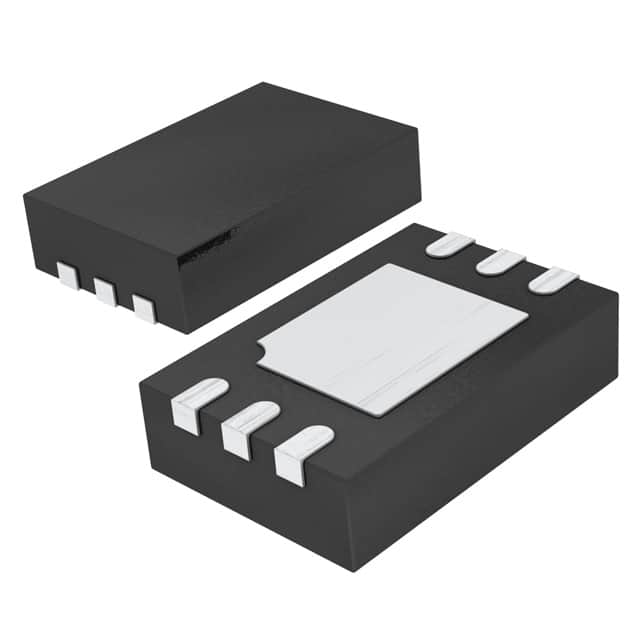
Package
The LTC6995CDCB-1#TRMPBF comes in a small form factor package, which is designed to be easily mounted on printed circuit boards (PCBs).
Essence
The essence of this product lies in its ability to generate precise and programmable clock signals, enabling accurate timing and synchronization in electronic systems.
Packaging/Quantity
The LTC6995CDCB-1#TRMPBF is typically packaged in reels or tubes, containing a specific quantity of ICs per package. The exact quantity may vary depending on the manufacturer's specifications.
Specifications
- Supply Voltage: 2.25V to 5.5V
- Frequency Range: Programmable from 488Hz to 2MHz
- Output Type: Square Wave
- Operating Temperature Range: -40°C to 85°C
- Package Type: 6-Lead DFN
Detailed Pin Configuration
The LTC6995CDCB-1#TRMPBF has the following pin configuration:
- GND (Ground)
- VCC (Supply Voltage)
- FREQ (Frequency Control Input)
- GATE (Gate Control Input)
- OUT (Output)
- NC (No Connection)
Functional Features
- Programmable frequency control allows for versatile timing applications.
- Wide supply voltage range enables compatibility with various power sources.
- Gate control input allows for external synchronization and signal gating.
- Square wave output provides a clean and easily interpretable clock signal.
Advantages
- High accuracy and stability ensure precise timing in electronic systems.
- Low power consumption contributes to energy efficiency.
- Wide operating temperature range allows for reliable performance in different environments.
- Small form factor package facilitates easy integration into PCB designs.
Disadvantages
- Limited frequency range may not be suitable for certain high-frequency applications.
- Lack of additional features, such as frequency modulation or phase control, may limit its use in more complex systems.
Working Principles
The LTC6995CDCB-1#TRMPBF utilizes an internal oscillator circuit that generates a square wave output. The frequency of the output signal is determined by the voltage applied to the FREQ pin. By programming this voltage, the desired frequency can be set within the specified range. The GATE pin allows for external control of the output signal, enabling synchronization or gating functionality.
Detailed Application Field Plans
The LTC6995CDCB-1#TRMPBF finds application in various fields, including:
- Timing circuits in microcontrollers and digital systems.
- Clock generation in communication devices and networks.
- Frequency control in test and measurement equipment.
- Synchronization in data acquisition systems.
- Pulse generation in industrial automation.
Detailed and Complete Alternative Models
- LTC6995CDCB-2#TRMPBF: Similar to LTC6995CDCB-1#TRMPBF but with extended frequency range.
- LTC6995CDCB-3#TRMPBF: Enhanced version with additional features like frequency modulation.
- LTC6995CDCB-4#TRMPBF: Higher precision variant with improved accuracy and stability.
These alternative models offer different specifications and features to cater to specific application requirements.
Word count: 518 words
Liệt kê 10 câu hỏi và câu trả lời thường gặp liên quan đến ứng dụng LTC6995CDCB-1#TRMPBF trong giải pháp kỹ thuật
Sure! Here are 10 common questions and answers related to the application of LTC6995CDCB-1#TRMPBF in technical solutions:
Q1: What is the LTC6995CDCB-1#TRMPBF? A1: The LTC6995CDCB-1#TRMPBF is a precision silicon oscillator with programmable frequency range and duty cycle. It is commonly used in various technical applications.
Q2: What is the operating voltage range of LTC6995CDCB-1#TRMPBF? A2: The operating voltage range of LTC6995CDCB-1#TRMPBF is from 2.25V to 5.5V.
Q3: How can I program the frequency range of LTC6995CDCB-1#TRMPBF? A3: The frequency range of LTC6995CDCB-1#TRMPBF can be programmed using external resistors and capacitors connected to its pins.
Q4: Can I adjust the duty cycle of the output signal generated by LTC6995CDCB-1#TRMPBF? A4: Yes, the duty cycle of the output signal can be adjusted using an external resistor connected to the SET pin of LTC6995CDCB-1#TRMPBF.
Q5: What is the typical frequency accuracy of LTC6995CDCB-1#TRMPBF? A5: The typical frequency accuracy of LTC6995CDCB-1#TRMPBF is ±0.5%.
Q6: Is LTC6995CDCB-1#TRMPBF suitable for battery-powered applications? A6: Yes, LTC6995CDCB-1#TRMPBF has a low operating voltage range and low power consumption, making it suitable for battery-powered applications.
Q7: Can I use LTC6995CDCB-1#TRMPBF in temperature-sensitive environments? A7: Yes, LTC6995CDCB-1#TRMPBF has a wide operating temperature range of -40°C to 125°C, making it suitable for temperature-sensitive environments.
Q8: What is the output signal format of LTC6995CDCB-1#TRMPBF? A8: The output signal of LTC6995CDCB-1#TRMPBF is a square wave.
Q9: Can I synchronize multiple LTC6995CDCB-1#TRMPBF devices together? A9: Yes, multiple LTC6995CDCB-1#TRMPBF devices can be synchronized by connecting their SYNC pins together.
Q10: Are there any evaluation boards available for LTC6995CDCB-1#TRMPBF? A10: Yes, Linear Technology (now part of Analog Devices) provides evaluation boards for LTC6995CDCB-1#TRMPBF, which can help in testing and prototyping applications.
Please note that these answers are general and may vary depending on specific application requirements. It is always recommended to refer to the datasheet and consult with the manufacturer for detailed information.