

Xem thông số kỹ thuật để biết chi tiết sản phẩm.
LFE2M50E-7F484C
Product Overview
Category
The LFE2M50E-7F484C belongs to the category of Field-Programmable Gate Arrays (FPGAs).
Use
This FPGA is commonly used in electronic circuits for various applications, including digital signal processing, communication systems, and embedded systems.
Characteristics
- High-performance programmable logic device
- Offers flexibility and reconfigurability
- Provides a large number of configurable logic blocks and input/output pins
- Supports complex designs and algorithms
- Low power consumption
- High-speed data processing capabilities
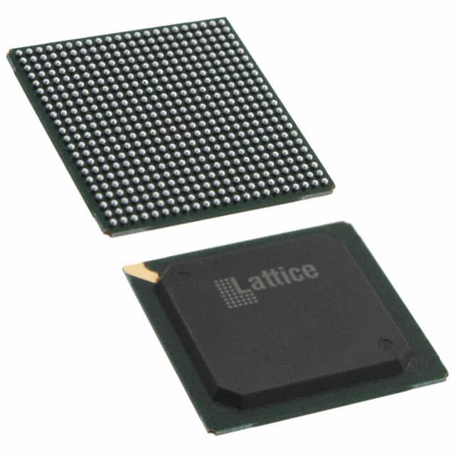
Package
The LFE2M50E-7F484C comes in a compact and durable package, ensuring easy integration into electronic systems. The package type is a 484-ball FineLine BGA (Ball Grid Array).
Essence
The essence of the LFE2M50E-7F484C lies in its ability to provide a customizable and versatile solution for implementing complex digital circuits.
Packaging/Quantity
Each package of LFE2M50E-7F484C contains one unit of the FPGA.
Specifications
- Logic Elements: 50,000
- Embedded Memory: 1,728 Kbits
- Maximum User I/Os: 316
- Block RAM: 2,304 Kbits
- Clock Management Tiles: 8
- Maximum Distributed RAM: 1,152 Kbits
- Maximum PLLs: 4
- Maximum Global Clock Networks: 16
Detailed Pin Configuration
The LFE2M50E-7F484C has a comprehensive pin configuration that allows for seamless integration into various electronic systems. The detailed pin configuration can be found in the product datasheet.
Functional Features
1. Flexibility and Reconfigurability
The LFE2M50E-7F484C offers a high degree of flexibility, allowing users to reconfigure the FPGA according to their specific requirements. This feature enables rapid prototyping and design iterations.
2. High-Speed Data Processing
With its high-performance architecture, the LFE2M50E-7F484C can process data at high speeds, making it suitable for applications that demand real-time processing capabilities.
3. Low Power Consumption
The FPGA is designed to minimize power consumption while maintaining optimal performance. This feature makes it ideal for battery-powered devices or energy-efficient applications.
4. Large Configurable Logic Blocks
The LFE2M50E-7F484C provides a significant number of configurable logic blocks, allowing designers to implement complex digital circuits efficiently.
Advantages and Disadvantages
Advantages
- Versatile and customizable solution for implementing complex digital circuits
- High-speed data processing capabilities
- Low power consumption
- Flexibility and reconfigurability for rapid prototyping
Disadvantages
- Relatively higher cost compared to other programmable logic devices
- Steeper learning curve for beginners due to its complexity
Working Principles
The LFE2M50E-7F484C operates based on the principles of field-programmable gate arrays. It consists of configurable logic blocks, interconnects, and input/output pins. The user can program the FPGA using hardware description languages (HDL) such as VHDL or Verilog. Once programmed, the FPGA executes the desired logic functions by routing signals through the configurable logic blocks and interconnects.
Detailed Application Field Plans
The LFE2M50E-7F484C finds extensive application in various fields, including:
Digital Signal Processing: The FPGA's high-speed data processing capabilities make it suitable for implementing advanced signal processing algorithms used in audio and video processing systems.
Communication Systems: The flexibility and reconfigurability of the FPGA enable its use in communication systems, such as wireless base stations, where it can handle complex modulation schemes and signal processing tasks.
Embedded Systems: The LFE2M50E-7F484C is widely used in embedded systems, including industrial automation, robotics, and automotive applications, where it provides the necessary computational power and flexibility for controlling and interfacing with various peripherals.
Detailed and Complete Alternative Models
LFE5UM5G-85F-8BG756I: This FPGA offers a higher logic capacity and enhanced performance compared to the LFE2M50E-7F484C. It is suitable for applications requiring more extensive computational resources.
LFE3-35EA-6FN672C: This FPGA provides a lower logic capacity but offers lower power consumption. It is ideal for battery-powered devices or applications with strict power constraints.
LCMXO2-1200HC-4TG100C: This low-cost FPGA is suitable for small-scale projects that require basic programmable logic capabilities. It is an
Liệt kê 10 câu hỏi và câu trả lời thường gặp liên quan đến ứng dụng LFE2M50E-7F484C trong giải pháp kỹ thuật
Sure! Here are 10 common questions and answers related to the application of LFE2M50E-7F484C in technical solutions:
Question: What is the LFE2M50E-7F484C?
Answer: The LFE2M50E-7F484C is a specific model of Field-Programmable Gate Array (FPGA) manufactured by Lattice Semiconductor.Question: What are the key features of the LFE2M50E-7F484C?
Answer: Some key features of this FPGA include 50,000 Look-Up Tables (LUTs), 4-input look-up tables, 1.2V core voltage, and 7ns typical delay.Question: What are the typical applications of the LFE2M50E-7F484C?
Answer: This FPGA can be used in various applications such as industrial automation, telecommunications, automotive systems, medical devices, and more.Question: How can I program the LFE2M50E-7F484C?
Answer: You can program this FPGA using the Lattice Diamond design software or other compatible programming tools provided by Lattice Semiconductor.Question: What is the maximum operating frequency of the LFE2M50E-7F484C?
Answer: The maximum operating frequency of this FPGA depends on the specific design and implementation, but it can typically reach frequencies of up to 300 MHz.Question: Can I interface the LFE2M50E-7F484C with other components or peripherals?
Answer: Yes, this FPGA supports various standard interfaces such as SPI, I2C, UART, and GPIO, allowing you to easily interface with other components or peripherals.Question: Does the LFE2M50E-7F484C support high-speed serial communication protocols?
Answer: Yes, this FPGA supports high-speed serial protocols like PCIe, SATA, and Ethernet, making it suitable for applications requiring fast data transfer.Question: What is the power consumption of the LFE2M50E-7F484C?
Answer: The power consumption of this FPGA depends on the specific design and usage scenario, but it typically operates at low power levels.Question: Can I use the LFE2M50E-7F484C in a battery-powered device?
Answer: Yes, this FPGA's low power consumption makes it suitable for battery-powered devices, as long as the power requirements are within the device's capabilities.Question: Are there any development boards or evaluation kits available for the LFE2M50E-7F484C?
Answer: Yes, Lattice Semiconductor provides development boards and evaluation kits specifically designed for the LFE2M50E-7F484C, which can help you get started with your designs quickly.
Please note that the answers provided here are general and may vary depending on the specific requirements and implementation of your technical solution.