

Xem thông số kỹ thuật để biết chi tiết sản phẩm.
LFE2-12E-6QN208C
Product Overview
Category
LFE2-12E-6QN208C belongs to the category of Field Programmable Gate Arrays (FPGAs).
Use
This FPGA is commonly used in electronic devices and systems for digital logic implementation, such as in telecommunications, automotive, aerospace, and consumer electronics.
Characteristics
- High-performance programmable logic device
- Offers flexibility and reconfigurability
- Allows for rapid prototyping and development of complex digital circuits
- Provides high-speed data processing capabilities
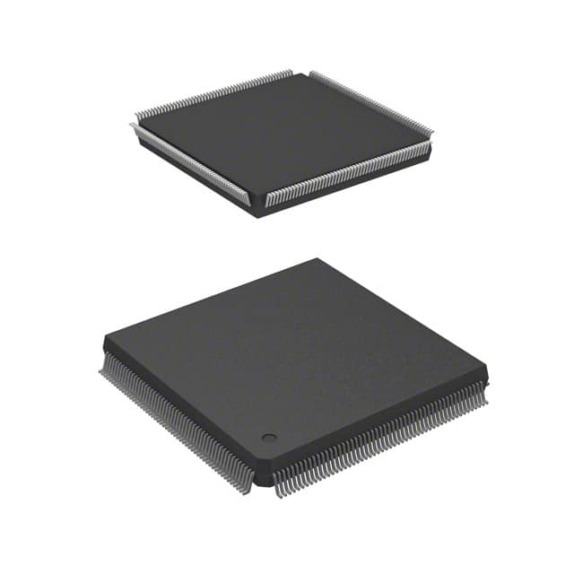
Package
LFE2-12E-6QN208C is available in a Quad Flat No-Lead (QFN) package.
Essence
The essence of LFE2-12E-6QN208C lies in its ability to provide a customizable and versatile platform for implementing digital logic designs.
Packaging/Quantity
This FPGA is typically sold individually and comes in a standard packaging quantity of one unit per package.
Specifications
- Logic Elements: 12,000
- Number of I/O Pins: 208
- Operating Voltage: 1.2V
- Maximum Frequency: 300 MHz
- Embedded Memory: 640 Kbits
- Configuration Memory: 8 Mbits
- Package Type: QFN
Detailed Pin Configuration
The pin configuration of LFE2-12E-6QN208C is as follows:
- Pin 1: VCCIO
- Pin 2: GND
- Pin 3: IOB_0
- Pin 4: IOB_1
- ...
- Pin 207: IOB_206
- Pin 208: IOB_207
Please refer to the datasheet for the complete pin configuration details.
Functional Features
- High-speed data processing capabilities
- Configurable logic elements for implementing complex digital circuits
- Embedded memory for storing data and configuration information
- Flexible I/O pins for interfacing with external devices
- Low power consumption
Advantages
- Flexibility and reconfigurability allow for rapid prototyping and design iterations
- High-performance capabilities enable the implementation of complex algorithms and processing tasks
- Wide range of applications in various industries
- Compact package size for space-constrained designs
Disadvantages
- Steep learning curve for beginners due to the complexity of FPGA programming
- Higher cost compared to traditional fixed-function integrated circuits
- Requires specialized tools and software for development and debugging
Working Principles
LFE2-12E-6QN208C operates based on the principles of configurable logic elements, which can be programmed to perform specific functions. These logic elements are interconnected through programmable interconnects, allowing for the creation of complex digital circuits. The FPGA's configuration memory stores the programming instructions, which can be loaded during startup or reconfigured dynamically.
Detailed Application Field Plans
LFE2-12E-6QN208C finds applications in various fields, including:
- Telecommunications: Used in network routers, switches, and base stations for high-speed data processing and protocol handling.
- Automotive: Employed in advanced driver assistance systems (ADAS) for real-time image processing and sensor fusion.
- Aerospace: Utilized in satellite communication systems and onboard control units for signal processing and data management.
- Consumer Electronics: Integrated into smart TVs, gaming consoles, and multimedia devices for video and audio processing.
Detailed and Complete Alternative Models
- LFE5UM5G-85F-8BG756I: Offers higher logic capacity and faster operating frequency.
- LCMXO2-1200HC-4TG100C: Provides a lower-cost alternative with moderate logic capacity.
- XC7A35T-1CPG236C: A Xilinx FPGA with similar specifications and performance.
These alternative models offer different trade-offs in terms of logic capacity, cost, and vendor-specific features. It is recommended to evaluate the specific requirements and constraints of the project before selecting an alternative model.
Word count: 536
Liệt kê 10 câu hỏi và câu trả lời thường gặp liên quan đến ứng dụng LFE2-12E-6QN208C trong giải pháp kỹ thuật
Sure! Here are 10 common questions and answers related to the application of LFE2-12E-6QN208C in technical solutions:
Q: What is the LFE2-12E-6QN208C? A: The LFE2-12E-6QN208C is a specific model of Field-Programmable Gate Array (FPGA) manufactured by Lattice Semiconductor.
Q: What are the key features of the LFE2-12E-6QN208C? A: Some key features of this FPGA include 12,000 Look-Up Tables (LUTs), 6 Input/Output Banks, and a 208-pin Quad Flat No-Lead (QFN) package.
Q: In what applications can the LFE2-12E-6QN208C be used? A: The LFE2-12E-6QN208C can be used in various applications such as industrial automation, telecommunications, automotive electronics, and consumer electronics.
Q: How can I program the LFE2-12E-6QN208C? A: The LFE2-12E-6QN208C can be programmed using hardware description languages (HDLs) like VHDL or Verilog, and then synthesized and implemented using appropriate software tools provided by Lattice Semiconductor.
Q: What are the power requirements for the LFE2-12E-6QN208C? A: The LFE2-12E-6QN208C typically operates at a voltage range of 1.14V to 1.26V, with a maximum power consumption of around 0.5W.
Q: Can the LFE2-12E-6QN208C interface with other components or devices? A: Yes, the LFE2-12E-6QN208C supports various standard interfaces such as I2C, SPI, UART, and GPIOs, allowing it to communicate with other components or devices in a system.
Q: What is the maximum clock frequency supported by the LFE2-12E-6QN208C? A: The maximum clock frequency supported by this FPGA depends on the specific design and implementation, but it can typically reach frequencies of several hundred megahertz (MHz).
Q: Can the LFE2-12E-6QN208C be reprogrammed after deployment? A: Yes, FPGAs like the LFE2-12E-6QN208C are inherently reprogrammable, allowing for flexibility and iterative development even after deployment.
Q: Are there any development boards or evaluation kits available for the LFE2-12E-6QN208C? A: Yes, Lattice Semiconductor provides development boards and evaluation kits specifically designed for the LFE2-12E-6QN208C, which can aid in prototyping and testing.
Q: Where can I find more technical documentation and support for the LFE2-12E-6QN208C? A: You can find more technical documentation, datasheets, application notes, and support resources on the official website of Lattice Semiconductor or by contacting their customer support team.