Xem thông số kỹ thuật để biết chi tiết sản phẩm.

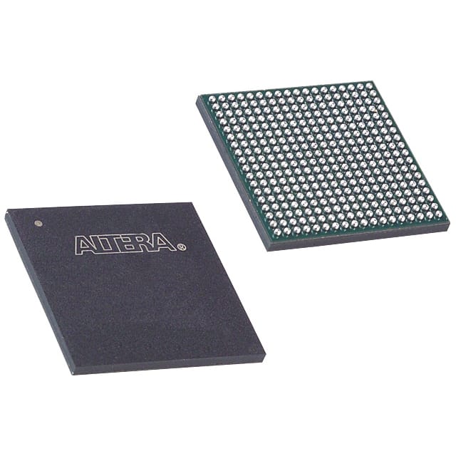
EP3C25F324I7
Product Overview
Category: Integrated Circuit (IC)
Use: The EP3C25F324I7 is a programmable logic device (PLD) that belongs to the Cyclone III family of Field-Programmable Gate Arrays (FPGAs). It is designed for various applications in the fields of telecommunications, automotive, industrial automation, and consumer electronics.
Characteristics: - High-performance FPGA with low power consumption - Offers high-speed data processing capabilities - Provides flexibility for customization and reconfiguration - Supports a wide range of I/O interfaces - Features embedded memory blocks for efficient data storage - Enables implementation of complex digital systems
Package: The EP3C25F324I7 comes in a compact 324-pin FineLine BGA package, which ensures reliable electrical connections and efficient heat dissipation.
Essence: This FPGA is built using advanced semiconductor technology, allowing users to program and configure its internal circuitry according to their specific requirements. It offers a versatile platform for designing and implementing complex digital systems.
Packaging/Quantity: The EP3C25F324I7 is typically sold individually in anti-static packaging to prevent damage during transportation and handling.
Specifications
- Logic Elements: 24,624
- Total RAM Bits: 1,288,800
- Maximum User I/Os: 202
- Embedded Multipliers: 56
- Maximum Operating Frequency: 300 MHz
- Supply Voltage: 1.2V
- Operating Temperature Range: -40°C to 100°C
Detailed Pin Configuration
The EP3C25F324I7 has a total of 324 pins, each serving a specific purpose in the overall functionality of the FPGA. A detailed pin configuration diagram can be found in the product datasheet.
Functional Features
- High-speed data processing: The EP3C25F324I7 offers fast data processing capabilities, making it suitable for applications that require real-time performance.
- Flexible configuration: Users can program and reconfigure the FPGA to implement various digital functions, allowing for customization and adaptability.
- Extensive I/O support: The device supports a wide range of I/O interfaces, enabling seamless integration with other components and systems.
- Embedded memory blocks: The FPGA includes embedded memory blocks, providing efficient storage for intermediate data and configuration settings.
- Low power consumption: The EP3C25F324I7 is designed to minimize power consumption, making it suitable for battery-powered devices.
Advantages and Disadvantages
Advantages: - Versatile and customizable platform for digital system design - High-performance data processing capabilities - Wide range of I/O interface support - Efficient use of embedded memory blocks - Low power consumption for energy-efficient applications
Disadvantages: - Limited logic elements compared to higher-end FPGAs - Relatively smaller number of user I/Os - Higher cost compared to simpler programmable logic devices
Working Principles
The EP3C25F324I7 operates based on the principles of field-programmable gate arrays. It consists of an array of configurable logic blocks (CLBs) interconnected through programmable interconnects. Users can program the internal circuitry of the FPGA using hardware description languages (HDLs) or graphical tools. Once programmed, the FPGA executes the desired digital functions by routing signals through the configured logic blocks.
Detailed Application Field Plans
The EP3C25F324I7 finds applications in various fields, including:
- Telecommunications: Used in network routers, switches, and communication equipment for high-speed data processing and protocol handling.
- Automotive: Employed in automotive electronics for control systems, infotainment, and driver assistance systems.
- Industrial Automation: Utilized in industrial control systems, robotics, and factory automation for real-time data processing and control.
- Consumer Electronics: Integrated into consumer devices such as gaming consoles, set-top boxes, and multimedia systems for high-performance multimedia processing.
Detailed and Complete Alternative Models
- EP3C16F484C6N: A lower-cost alternative with fewer logic elements and I/Os, suitable for simpler applications.
- EP4CE22F17C8N: A higher-end FPGA with more logic elements and I/Os, offering increased processing power and flexibility.
- EP2C35F672C6: An alternative model from a different FPGA family, providing similar capabilities but with a different pin configuration.
These alternative models cater to different application requirements and budget constraints, allowing users to choose the most suitable FPGA for their specific needs.
Word count: 610 words
Liệt kê 10 câu hỏi và câu trả lời thường gặp liên quan đến ứng dụng EP3C25F324I7 trong giải pháp kỹ thuật
Sure! Here are 10 common questions and answers related to the application of EP3C25F324I7 in technical solutions:
Q: What is EP3C25F324I7? A: EP3C25F324I7 is a field-programmable gate array (FPGA) manufactured by Intel (formerly Altera). It is designed for various digital logic applications.
Q: What are the key features of EP3C25F324I7? A: Some key features include 25,000 logic elements, 324 user I/O pins, embedded memory blocks, PLLs, and support for various communication protocols.
Q: What are the typical applications of EP3C25F324I7? A: EP3C25F324I7 can be used in a wide range of applications such as industrial automation, telecommunications, automotive systems, medical devices, and high-performance computing.
Q: How can EP3C25F324I7 be programmed? A: EP3C25F324I7 can be programmed using hardware description languages (HDLs) like VHDL or Verilog, which describe the desired functionality of the FPGA.
Q: Can EP3C25F324I7 interface with other components or devices? A: Yes, EP3C25F324I7 supports various communication protocols like UART, SPI, I2C, and Ethernet, allowing it to interface with other components or devices.
Q: Is EP3C25F324I7 suitable for real-time applications? A: Yes, EP3C25F324I7 can be used in real-time applications due to its high-speed performance and ability to handle complex logic operations efficiently.
Q: Can EP3C25F324I7 be reprogrammed after deployment? A: Yes, EP3C25F324I7 is a reprogrammable FPGA, which means its configuration can be changed even after it has been deployed in a system.
Q: What development tools are available for programming EP3C25F324I7? A: Intel Quartus Prime is the primary development tool used to program and configure EP3C25F324I7. It provides a complete design environment for FPGA development.
Q: Are there any limitations or considerations when using EP3C25F324I7? A: Some considerations include power consumption, heat dissipation, and the need for proper signal integrity and timing analysis during the design phase.
Q: Where can I find additional resources and support for EP3C25F324I7? A: Intel (formerly Altera) provides comprehensive documentation, application notes, reference designs, and technical support on their website for EP3C25F324I7.
Please note that these answers are general and may vary depending on specific requirements and use cases.

