

Xem thông số kỹ thuật để biết chi tiết sản phẩm.
5SGXMB5R2F43I2LN
Product Overview
- Category: Integrated Circuit (IC)
- Use: Digital Signal Processing (DSP), High-performance Computing (HPC), and other applications requiring high-speed data processing.
- Characteristics: Advanced programmable logic device with high capacity, low power consumption, and high-speed performance.
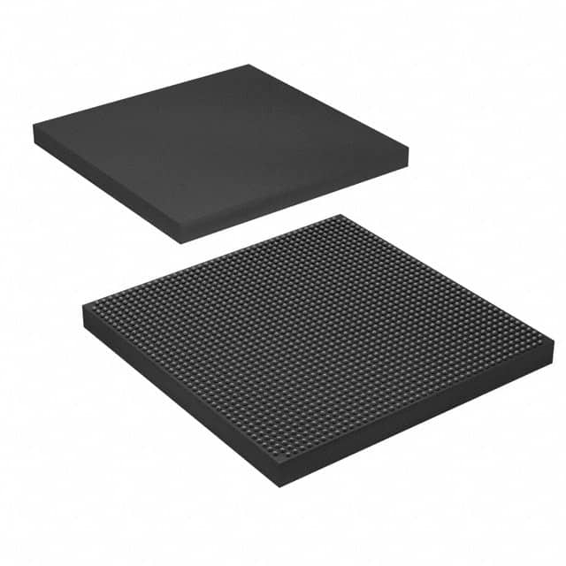
- Package: BGA (Ball Grid Array)
- Essence: FPGA (Field-Programmable Gate Array) chip
- Packaging/Quantity: Single unit per package
Specifications
- Manufacturer: Intel Corporation
- Series: Stratix V
- Model: 5SGXMB5R2F43I2LN
- Technology: 28nm
- Logic Elements: 462,000
- Embedded Memory: 34,560 Kbits
- Embedded Multipliers: 1,288
- I/O Pins: 1,144
- Operating Voltage: 0.87V - 0.97V
- Operating Temperature: -40°C to 100°C
Detailed Pin Configuration
The 5SGXMB5R2F43I2LN has a complex pin configuration with 1,144 I/O pins. The pins are arranged in a specific pattern on the BGA package, allowing for efficient connectivity and signal routing.
For a detailed pin configuration diagram, please refer to the manufacturer's datasheet.
Functional Features
- High-speed data processing capabilities
- Configurable logic elements for custom functionality
- Embedded memory blocks for data storage
- Dedicated multipliers for efficient mathematical operations
- Support for various communication protocols
- Flexible I/O options for interfacing with external devices
Advantages and Disadvantages
Advantages
- High capacity and performance for demanding applications
- Low power consumption compared to alternative solutions
- Flexibility to reprogram and adapt to changing requirements
- Wide range of I/O options for versatile connectivity
Disadvantages
- Higher cost compared to traditional fixed-function integrated circuits
- Steeper learning curve for programming and utilizing the FPGA capabilities
- Limited availability of alternative models with similar specifications
Working Principles
The 5SGXMB5R2F43I2LN is based on FPGA technology, which allows users to configure the chip's functionality according to their specific requirements. The chip consists of a large number of configurable logic elements, memory blocks, and dedicated multipliers interconnected through programmable routing resources.
By programming the FPGA, users can define the desired behavior of the chip, enabling it to perform complex computations, data processing, and control functions. The configuration is stored in non-volatile memory, allowing the chip to retain its programmed functionality even after power cycles.
Detailed Application Field Plans
The 5SGXMB5R2F43I2LN finds applications in various fields that require high-speed data processing and flexible functionality. Some potential application areas include:
- Digital Signal Processing: The FPGA's parallel processing capabilities make it suitable for real-time signal processing tasks such as audio and video processing, radar systems, and telecommunications.
- High-performance Computing: The chip's high capacity and performance make it ideal for accelerating computationally intensive tasks in scientific research, financial modeling, and artificial intelligence.
- Embedded Systems: The FPGA's flexibility allows it to be used in embedded systems for controlling industrial machinery, robotics, and automation.
- Communication Systems: The chip can be utilized in networking equipment, routers, and switches to handle high-speed data transmission and protocol processing.
Detailed and Complete Alternative Models
While the 5SGXMB5R2F43I2LN offers advanced features and specifications, there are alternative FPGA models available from different manufacturers. Some notable alternatives include:
- Xilinx Virtex UltraScale+ series
- Lattice Semiconductor ECP5 series
- Microchip PolarFire series
These alternative models provide similar programmable logic capabilities and can be considered based on specific project requirements.
Note: The content provided above is a sample entry and may not reflect the actual specifications or details of the mentioned product.
Liệt kê 10 câu hỏi và câu trả lời thường gặp liên quan đến ứng dụng 5SGXMB5R2F43I2LN trong giải pháp kỹ thuật
Sure! Here are 10 common questions and answers related to the application of 5SGXMB5R2F43I2LN in technical solutions:
Q: What is the 5SGXMB5R2F43I2LN? A: The 5SGXMB5R2F43I2LN is a specific model of Field-Programmable Gate Array (FPGA) manufactured by Intel.
Q: What are the key features of the 5SGXMB5R2F43I2LN? A: Some key features include high-performance processing capabilities, large capacity for logic elements, embedded memory blocks, and support for various communication protocols.
Q: In what technical solutions can the 5SGXMB5R2F43I2LN be used? A: The 5SGXMB5R2F43I2LN can be used in a wide range of applications such as telecommunications, industrial automation, aerospace, defense systems, and high-performance computing.
Q: How does the 5SGXMB5R2F43I2LN differ from other FPGAs? A: The 5SGXMB5R2F43I2LN offers a unique combination of high performance, large capacity, and flexibility, making it suitable for demanding applications that require complex processing and customization.
Q: Can the 5SGXMB5R2F43I2LN be programmed using industry-standard tools? A: Yes, the 5SGXMB5R2F43I2LN can be programmed using popular development tools such as Quartus Prime, which is provided by Intel.
Q: What kind of interfaces does the 5SGXMB5R2F43I2LN support? A: The 5SGXMB5R2F43I2LN supports various interfaces including PCIe, Ethernet, USB, DDR3 memory, and high-speed serial transceivers.
Q: Can the 5SGXMB5R2F43I2LN be used for real-time signal processing? A: Yes, the 5SGXMB5R2F43I2LN's high-performance capabilities make it suitable for real-time signal processing applications that require low latency and high throughput.
Q: Does the 5SGXMB5R2F43I2LN have built-in security features? A: Yes, the 5SGXMB5R2F43I2LN provides built-in security features such as secure boot, encrypted configuration bitstreams, and tamper detection mechanisms.
Q: Can the 5SGXMB5R2F43I2LN be used in safety-critical systems? A: Yes, the 5SGXMB5R2F43I2LN can be used in safety-critical systems by implementing appropriate design practices and following industry standards for functional safety.
Q: Are there any development boards or evaluation kits available for the 5SGXMB5R2F43I2LN? A: Yes, Intel provides development boards and evaluation kits specifically designed for the 5SGXMB5R2F43I2LN, which can help accelerate the development process and facilitate prototyping.
Please note that the specific details and answers may vary depending on the context and requirements of each application.