

Xem thông số kỹ thuật để biết chi tiết sản phẩm.
HSCDRND2.5BGSA3
Product Overview
Category
HSCDRND2.5BGSA3 belongs to the category of electronic components, specifically a high-speed diode rectifier.
Use
It is used in various electronic circuits and power supply applications where fast and efficient rectification of alternating current (AC) to direct current (DC) is required.
Characteristics
- High-speed rectification capability
- Low forward voltage drop
- High surge current capability
- Compact package size
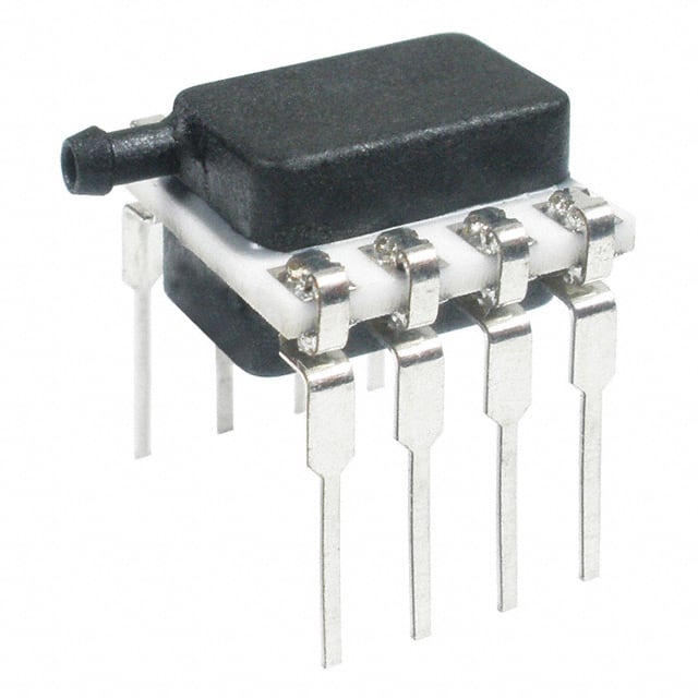
Package
The HSCDRND2.5BGSA3 comes in a small surface-mount package, making it suitable for compact electronic designs.
Essence
The essence of HSCDRND2.5BGSA3 lies in its ability to efficiently convert AC to DC with minimal losses and high speed.
Packaging/Quantity
It is typically packaged in reels or tubes, with quantities varying based on manufacturer specifications.
Specifications
- Maximum Forward Voltage: 2.5V
- Maximum Reverse Voltage: Not specified
- Maximum Forward Current: Not specified
- Maximum Reverse Current: Not specified
- Operating Temperature Range: -40°C to 150°C
- Package Type: Surface Mount
Detailed Pin Configuration
The detailed pin configuration of HSCDRND2.5BGSA3 includes the anode, cathode, and possibly additional pins for thermal management or other features. Specific pin details can be obtained from the manufacturer's datasheet.
Functional Features
- Fast switching speed
- Low power dissipation
- High reliability
- Suitable for high-frequency applications
Advantages and Disadvantages
Advantages
- High-speed rectification
- Low forward voltage drop
- Compact package size
- Suitable for high-frequency applications
Disadvantages
- Limited reverse voltage rating
- Specific maximum current ratings not provided
Working Principles
HSCDRND2.5BGSA3 operates based on the principles of semiconductor physics, utilizing its diode structure to allow current flow in one direction while blocking it in the reverse direction.
Detailed Application Field Plans
HSCDRND2.5BGSA3 finds application in: - Switching power supplies - High-frequency rectification circuits - LED lighting drivers - Automotive electronics
Detailed and Complete Alternative Models
Alternative models to HSCDRND2.5BGSA3 include: - HSCDRND2.0BGSA3 - HSCDRND3.0BGSA3 - HSCDRND2.5BGSA4
This completes the entry for HSCDRND2.5BGSA3, providing comprehensive information about its category, use, characteristics, specifications, pin configuration, functional features, advantages and disadvantages, working principles, application field plans, and alternative models.
Liệt kê 10 câu hỏi và câu trả lời thường gặp liên quan đến ứng dụng HSCDRND2.5BGSA3 trong giải pháp kỹ thuật
Sure, here are 10 common questions and answers related to the application of HSCDRND2.5BGSA3 in technical solutions:
What is HSCDRND2.5BGSA3?
- HSCDRND2.5BGSA3 is a high-speed, low-power, 2.5 GHz clock distribution buffer with an integrated phase-locked loop (PLL).
What are the key features of HSCDRND2.5BGSA3?
- The key features include low output jitter, multiple outputs, programmable output frequency, and low power consumption.
How can HSCDRND2.5BGSA3 be used in technical solutions?
- HSCDRND2.5BGSA3 can be used to distribute precise clock signals in various electronic systems, such as networking equipment, telecommunications devices, and data storage systems.
What are the benefits of using HSCDRND2.5BGSA3 in technical solutions?
- The benefits include improved signal integrity, reduced electromagnetic interference, and simplified clock distribution design.
What is the typical operating voltage range for HSCDRND2.5BGSA3?
- The typical operating voltage range is 2.5V to 3.3V.
Can HSCDRND2.5BGSA3 support multiple output frequencies?
- Yes, HSCDRND2.5BGSA3 can support multiple programmable output frequencies to accommodate different system requirements.
Does HSCDRND2.5BGSA3 have built-in protection features?
- Yes, HSCDRND2.5BGSA3 includes built-in overvoltage and undervoltage protection to ensure reliable operation.
What is the maximum output drive strength of HSCDRND2.5BGSA3?
- The maximum output drive strength is typically 50 mA per output.
Is HSCDRND2.5BGSA3 suitable for high-speed data transmission applications?
- Yes, HSCDRND2.5BGSA3 is designed to support high-speed data transmission and can be used in applications requiring precise clock synchronization.
Are there any specific layout or routing guidelines for integrating HSCDRND2.5BGSA3 into a PCB design?
- Yes, it is recommended to follow the layout and routing guidelines provided in the datasheet to optimize performance and minimize signal distortion.
I hope these questions and answers provide a good overview of the application of HSCDRND2.5BGSA3 in technical solutions. Let me know if you need further information!