

Xem thông số kỹ thuật để biết chi tiết sản phẩm.
Encyclopedia Entry: 74AUP1G08FW5-7
Product Overview
Category
The 74AUP1G08FW5-7 belongs to the category of integrated circuits (ICs) and specifically falls under the logic gates subcategory.
Use
This product is commonly used in digital electronics for logical operations. It serves as a single 2-input AND gate, allowing for the combination of two binary inputs to produce an output based on the logical AND operation.
Characteristics
- Low power consumption: The 74AUP1G08FW5-7 operates at low voltage levels, resulting in reduced power consumption.
- High-speed operation: This IC offers fast switching times, enabling efficient processing of logical operations.
- Small form factor: The compact size of the 74AUP1G08FW5-7 makes it suitable for applications with limited space constraints.
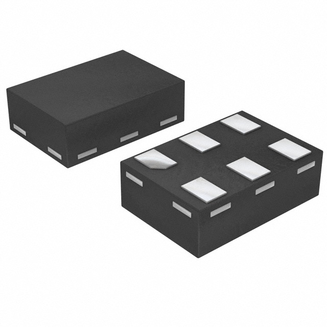
Package
The 74AUP1G08FW5-7 is available in a small surface-mount package, typically referred to as a SOT353 or SC-88A. This package ensures easy integration onto circuit boards and facilitates mass production.
Essence
The essence of the 74AUP1G08FW5-7 lies in its ability to perform logical AND operations, making it a fundamental component in digital systems.
Packaging/Quantity
The 74AUP1G08FW5-7 is commonly packaged in reels or tape and reel packaging. Each reel typically contains 3000 units, ensuring sufficient quantities for various applications.
Specifications
- Supply Voltage Range: 0.8V to 3.6V
- Input Voltage Range: 0V to VCC
- Output Voltage Range: 0V to VCC
- Operating Temperature Range: -40°C to +85°C
- Maximum Propagation Delay: 4.5ns (at 3.3V)
- Maximum Quiescent Current: 1μA (at 3.3V)
Detailed Pin Configuration
The 74AUP1G08FW5-7 features a total of 5 pins, each serving a specific purpose:
- Pin 1 (A): Input A
- Pin 2 (B): Input B
- Pin 3 (GND): Ground
- Pin 4 (Y): Output Y
- Pin 5 (VCC): Power Supply
Functional Features
The key functional features of the 74AUP1G08FW5-7 include:
- AND gate operation: The IC performs the logical AND operation on the inputs A and B, generating the corresponding output Y.
- Schmitt-trigger input: The device incorporates a Schmitt-trigger input, ensuring robust and noise-tolerant operation.
- Wide voltage range: The IC supports a wide supply voltage range, allowing compatibility with various digital systems.
Advantages and Disadvantages
Advantages
- Low power consumption enables energy-efficient designs.
- High-speed operation facilitates rapid data processing.
- Small form factor allows for space-saving integration.
- Schmitt-trigger input ensures reliable performance in noisy environments.
Disadvantages
- Limited to 2-input AND gate functionality, restricting its application to specific logic operations.
- Not suitable for applications requiring more complex logical operations.
Working Principles
The 74AUP1G08FW5-7 operates based on the principles of Boolean logic. It utilizes transistors and other electronic components to implement the logical AND function. When both inputs A and B are high (logic level 1), the output Y will be high. Otherwise, the output remains low (logic level 0).
Detailed Application Field Plans
The 74AUP1G08FW5-7 finds extensive application in various digital systems, including but not limited to:
- Microcontrollers and microprocessors
- Communication devices (e.g., routers, switches)
- Consumer electronics (e.g., smartphones, tablets)
- Industrial automation systems
- Automotive electronics
Detailed and Complete Alternative Models
Several alternative models with similar functionality to the 74AUP1G08FW5-7 include:
- SN74LVC1G08: Manufactured by Texas Instruments
- MC74VHC1G08: Manufactured by ON Semiconductor
- 74HC08: Manufactured by NXP Semiconductors
These alternatives offer comparable performance and can be used as substitutes for the 74AUP1G08FW5-7 in various applications.
In conclusion, the 74AUP1G08FW5-7 is a low-power, high-speed logic gate IC that performs the logical AND operation. Its compact size, wide voltage range, and Schmitt-trigger input make it suitable for numerous digital applications. While it has limitations in terms of functionality, alternative models are available to cater to specific
Liệt kê 10 câu hỏi và câu trả lời thường gặp liên quan đến ứng dụng 74AUP1G08FW5-7 trong giải pháp kỹ thuật
Sure! Here are 10 common questions and answers related to the application of the 74AUP1G08FW5-7 in technical solutions:
Q1: What is the 74AUP1G08FW5-7? A1: The 74AUP1G08FW5-7 is a single 2-input AND gate that operates at a voltage range of 0.8V to 3.6V.
Q2: What is the purpose of an AND gate? A2: An AND gate is a digital logic gate that outputs a high signal only when both of its inputs are high.
Q3: What are the typical applications of the 74AUP1G08FW5-7? A3: The 74AUP1G08FW5-7 can be used in various applications such as battery-powered devices, portable electronics, industrial automation, and communication systems.
Q4: What is the maximum operating frequency of the 74AUP1G08FW5-7? A4: The maximum operating frequency of the 74AUP1G08FW5-7 is typically around 500 MHz.
Q5: What is the power supply voltage range for this device? A5: The 74AUP1G08FW5-7 operates within a power supply voltage range of 0.8V to 3.6V.
Q6: Can I use this gate with a higher voltage supply? A6: No, the 74AUP1G08FW5-7 is designed to operate within the specified voltage range and should not be used with a higher voltage supply.
Q7: What is the input voltage threshold for this gate? A7: The input voltage threshold for the 74AUP1G08FW5-7 is typically around 0.7V.
Q8: Can I use this gate in a mixed-voltage system? A8: Yes, the 74AUP1G08FW5-7 is compatible with mixed-voltage systems as it can operate at different voltage levels.
Q9: What is the output drive capability of this gate? A9: The 74AUP1G08FW5-7 has a typical output drive capability of 32 mA.
Q10: Is this gate available in different package options? A10: Yes, the 74AUP1G08FW5-7 is available in various package options such as SOT353 and XSON6.