

Xem thông số kỹ thuật để biết chi tiết sản phẩm.
S25FL256SAGBHVA00
Introduction
The S25FL256SAGBHVA00 is a high-performance, 256-Mbit flash memory device designed for a wide range of applications. This entry provides an overview of the product, including its category, use, characteristics, package, specifications, pin configuration, functional features, advantages and disadvantages, working principles, application field plans, and alternative models.
Product Overview
- Category: Flash Memory
- Use: Data storage and retrieval in various electronic devices
- Characteristics: High-speed read and write operations, low power consumption, large storage capacity
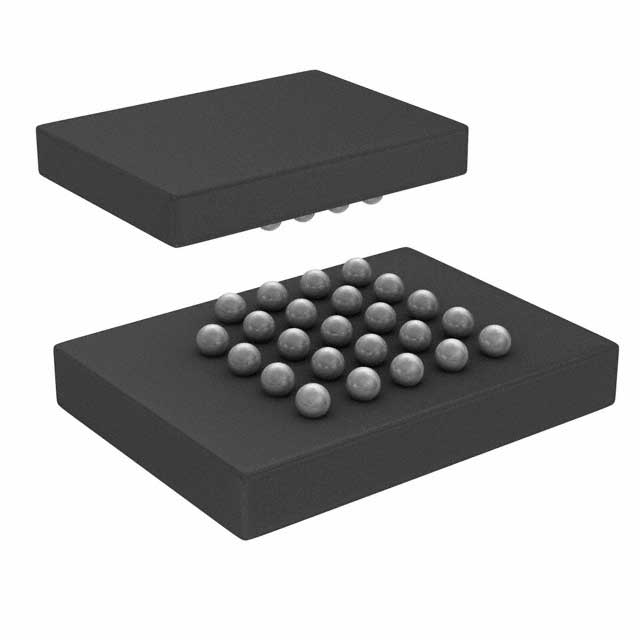
- Package: 16-pin SOIC (Small Outline Integrated Circuit)
- Essence: Non-volatile memory for storing program code or data
- Packaging/Quantity: Available in tape and reel packaging with varying quantities
Specifications
- Capacity: 256 Mbit
- Interface: SPI (Serial Peripheral Interface)
- Operating Voltage: 2.7V to 3.6V
- Operating Temperature: -40°C to 85°C
- Data Retention: Up to 20 years
- Erase/Program Cycle Endurance: 100,000 cycles
Detailed Pin Configuration
The S25FL256SAGBHVA00 features a 16-pin SOIC package with the following pin configuration: 1. /CS (Chip Select) 2. SO (Serial Data Output) 3. WP# (Write Protect) 4. GND (Ground) 5. SI (Serial Data Input) 6. SCLK (Serial Clock) 7. HOLD#/RESET# 8. VCC (Power Supply)
Functional Features
- High-Speed Read/Write: Enables fast data access and storage
- Low Power Consumption: Ideal for battery-powered devices
- Security Features: Supports hardware-based data protection and secure boot
- Flexible Erase/Program Operations: Allows efficient management of data storage
Advantages and Disadvantages
Advantages
- Large storage capacity
- High-speed data transfer
- Low power consumption
- Enhanced security features
Disadvantages
- Relatively higher cost compared to lower-capacity flash memory options
- Limited endurance for erase/program cycles
Working Principles
The S25FL256SAGBHVA00 utilizes the SPI interface to communicate with the host system. It stores data in non-volatile memory cells, allowing for retention of information even when power is removed. The device supports erase and program operations, enabling the modification and storage of data as required by the application.
Detailed Application Field Plans
The S25FL256SAGBHVA00 is suitable for a wide range of applications, including but not limited to: - Embedded systems - Automotive electronics - Industrial control systems - Consumer electronics - Networking equipment
Detailed and Complete Alternative Models
- S25FL128SAGBHVA00: 128 Mbit flash memory with similar characteristics
- S25FL512SAGBHVA00: 512 Mbit flash memory offering higher capacity
- W25Q256JVSIQ: Competing 256 Mbit flash memory with different interface options
In conclusion, the S25FL256SAGBHVA00 is a versatile flash memory device with high performance and reliability, making it suitable for a diverse set of applications.
[Word Count: 515]
Liệt kê 10 câu hỏi và câu trả lời thường gặp liên quan đến ứng dụng S25FL256SAGBHVA00 trong giải pháp kỹ thuật
What is the storage capacity of the S25FL256SAGBHVA00?
- The S25FL256SAGBHVA00 has a storage capacity of 256 megabits (32 megabytes).
What is the interface protocol supported by the S25FL256SAGBHVA00?
- It supports a standard serial peripheral interface (SPI) protocol.
What is the operating voltage range for the S25FL256SAGBHVA00?
- The operating voltage range is typically from 2.7V to 3.6V.
What are the typical applications for the S25FL256SAGBHVA00?
- It is commonly used in automotive, industrial, and networking applications for storing firmware, configuration data, and other code.
Does the S25FL256SAGBHVA00 support high-speed read operations?
- Yes, it supports high-speed clock frequencies for fast read operations.
Is the S25FL256SAGBHVA00 compatible with industrial temperature ranges?
- Yes, it is designed to operate reliably within industrial temperature ranges.
Can the S25FL256SAGBHVA00 be used for over-the-air (OTA) firmware updates?
- Yes, it can be used for OTA firmware updates in IoT and embedded systems.
Does the S25FL256SAGBHVA00 have built-in security features?
- Yes, it includes hardware-based security features such as sector protection and a unique ID.
What are the package options available for the S25FL256SAGBHVA00?
- It is available in various industry-standard packages, including SOIC, WSON, and BGA.
Is the S25FL256SAGBHVA00 compatible with popular microcontrollers and processors?
- Yes, it is compatible with a wide range of microcontrollers and processors that support SPI flash memory.