

Xem thông số kỹ thuật để biết chi tiết sản phẩm.
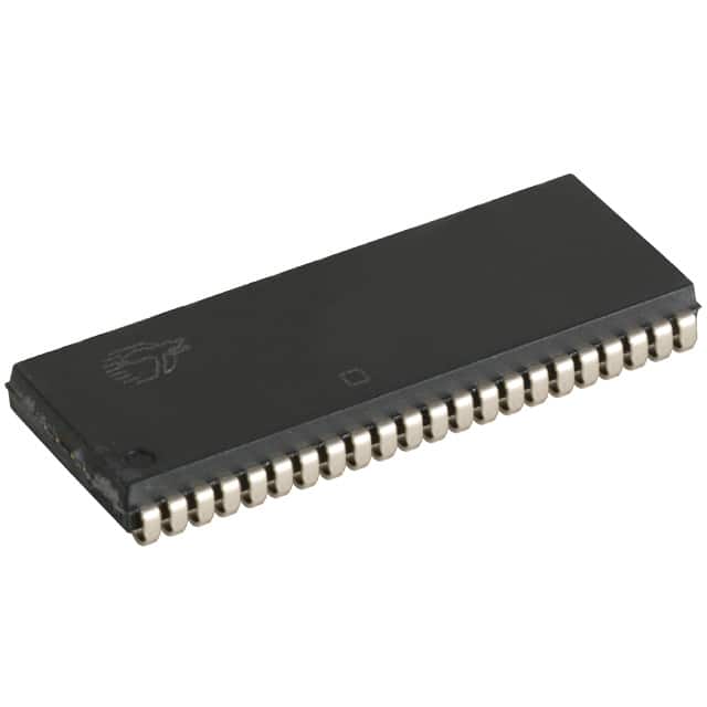
CY7C1041GE-10VXI
Basic Information Overview
- Category: Integrated Circuit (IC)
- Use: Memory chip
- Characteristics: High-speed, low-power, synchronous SRAM
- Package: 32-pin Very Small Outline Integrated Circuit (VSOP)
- Essence: Stores and retrieves digital information in electronic devices
- Packaging/Quantity: Typically sold in reels of 250 units
Specifications
- Operating Voltage: 3.3V
- Access Time: 10ns
- Density: 4 Megabits (512K x 8)
- Organization: 512K words x 8 bits
- Interface: Parallel
- Clock Frequency: 100MHz
- Power Consumption: Low power operation with standby mode
Detailed Pin Configuration
The CY7C1041GE-10VXI has a total of 32 pins, which are assigned specific functions. The pin configuration is as follows:
| Pin Number | Pin Name | Function | |------------|----------|----------| | 1 | VCC | Power supply voltage | | 2 | A0 | Address input bit 0 | | 3 | A1 | Address input bit 1 | | 4 | A2 | Address input bit 2 | | 5 | A3 | Address input bit 3 | | 6 | A4 | Address input bit 4 | | 7 | A5 | Address input bit 5 | | 8 | A6 | Address input bit 6 | | 9 | A7 | Address input bit 7 | | 10 | A8 | Address input bit 8 | | 11 | A9 | Address input bit 9 | | 12 | A10 | Address input bit 10 | | 13 | A11 | Address input bit 11 | | 14 | A12 | Address input bit 12 | | 15 | A13 | Address input bit 13 | | 16 | A14 | Address input bit 14 | | 17 | A15 | Address input bit 15 | | 18 | CE1 | Chip Enable 1 (Active Low) | | 19 | CE2 | Chip Enable 2 (Active Low) | | 20 | WE | Write Enable (Active Low) | | 21 | OE | Output Enable (Active Low) | | 22-29 | DQ0-DQ7 | Data Input/Output | | 30 | VSS | Ground | | 31 | NC | No Connection | | 32 | VCCQ | Power supply voltage for output buffers |
Functional Features
- High-speed operation: The CY7C1041GE-10VXI offers a fast access time of 10ns, allowing for quick data retrieval.
- Low power consumption: This memory chip is designed to operate with low power consumption, making it suitable for battery-powered devices.
- Synchronous operation: The chip synchronizes its operations with an external clock signal, ensuring reliable and accurate data transfer.
- Easy integration: The parallel interface simplifies the integration of the chip into various electronic systems.
Advantages and Disadvantages
Advantages: - High-speed operation enables efficient data processing. - Low power consumption prolongs battery life in portable devices. - Synchronous operation ensures reliable data transfer. - Easy integration into different electronic systems.
Disadvantages: - Limited storage capacity compared to higher-density memory chips. - Parallel interface may require more complex circuitry for interfacing with modern microcontrollers.
Working Principles
The CY7C1041GE-10VXI is a synchronous static random-access memory (SRAM) chip. It stores digital information in a volatile manner, meaning the data is lost when power is removed. The chip operates by receiving address inputs to select specific memory locations and transferring data through the parallel interface. The synchronous operation ensures that data is read or written accurately based on the timing provided by an external clock signal.
Detailed Application Field Plans
The CY7C1041GE-10VXI can be used in various applications, including: 1. Computer systems: Used as cache memory for faster data access. 2. Networking devices: Provides temporary storage for packet processing. 3. Industrial control systems: Stores critical data for real-time monitoring and control. 4. Consumer electronics: Used in gaming consoles, set-top boxes, and other devices requiring fast data access.
Detailed and Complete Alternative Models
- CY7C1041GN-10VXI: Similar specifications but with a different package type (TSOP).
- CY7C1041DV33-10VXI: Same specifications
Liệt kê 10 câu hỏi và câu trả lời thường gặp liên quan đến ứng dụng CY7C1041GE-10VXI trong giải pháp kỹ thuật
Sure! Here are 10 common questions and answers related to the application of CY7C1041GE-10VXI in technical solutions:
Q1: What is the CY7C1041GE-10VXI? A1: The CY7C1041GE-10VXI is a high-speed, low-power, 4-megabit (256K x 16) CMOS static RAM (SRAM) device.
Q2: What are the key features of CY7C1041GE-10VXI? A2: Some key features include a fast access time of 10 ns, low power consumption, wide voltage range (3.0V to 3.6V), and a small form factor.
Q3: What are some typical applications for CY7C1041GE-10VXI? A3: CY7C1041GE-10VXI can be used in various applications such as networking equipment, telecommunications systems, industrial automation, and embedded systems.
Q4: What is the operating voltage range for CY7C1041GE-10VXI? A4: The operating voltage range for CY7C1041GE-10VXI is 3.0V to 3.6V.
Q5: What is the maximum operating frequency of CY7C1041GE-10VXI? A5: The maximum operating frequency of CY7C1041GE-10VXI is typically 100 MHz.
Q6: Does CY7C1041GE-10VXI support multiple read and write operations simultaneously? A6: Yes, CY7C1041GE-10VXI supports multiple read and write operations simultaneously.
Q7: Can CY7C1041GE-10VXI operate in harsh environments? A7: CY7C1041GE-10VXI is designed to operate in industrial temperature ranges (-40°C to +85°C), making it suitable for harsh environments.
Q8: What is the power consumption of CY7C1041GE-10VXI? A8: The power consumption of CY7C1041GE-10VXI is low, making it energy-efficient for battery-powered applications.
Q9: Does CY7C1041GE-10VXI have any built-in error correction capabilities? A9: No, CY7C1041GE-10VXI does not have built-in error correction capabilities. External error correction techniques may be required if needed.
Q10: Can CY7C1041GE-10VXI be easily integrated into existing designs? A10: Yes, CY7C1041GE-10VXI is available in a standard 44-pin TSOP package, which makes it compatible with many existing designs and easy to integrate.
Please note that these answers are general and may vary depending on specific requirements and use cases.