

Xem thông số kỹ thuật để biết chi tiết sản phẩm.
CY7C0241E-25AXC
Product Overview
Category
The CY7C0241E-25AXC belongs to the category of integrated circuits (ICs).
Use
This IC is commonly used in electronic devices for various applications, including data storage, communication systems, and digital signal processing.
Characteristics
- High-speed performance: The CY7C0241E-25AXC operates at a high clock frequency, enabling fast data transfer and processing.
- Low power consumption: This IC is designed to minimize power consumption, making it suitable for battery-powered devices.
- Wide operating voltage range: It can operate within a wide voltage range, providing flexibility in different electronic systems.
- Small form factor: The CY7C0241E-25AXC is available in a compact package, allowing for space-efficient integration into electronic designs.
Package and Quantity
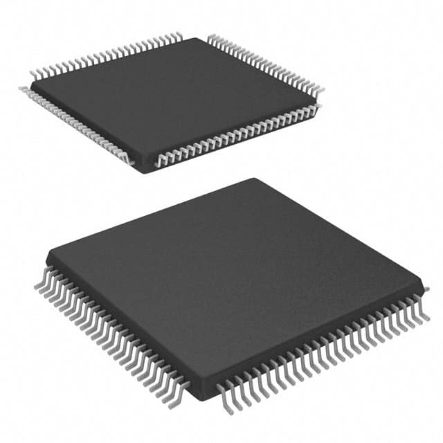
The CY7C0241E-25AXC is packaged in a small outline integrated circuit (SOIC) package. It is typically sold in reels or tubes containing a specific quantity, such as 250 or 1000 units per package.
Specifications
- Operating Voltage: 2.7V - 3.6V
- Clock Frequency: Up to 25 MHz
- Data Transfer Rate: 200 Mbps
- Operating Temperature Range: -40°C to +85°C
- Pin Count: 32
Detailed Pin Configuration
The CY7C0241E-25AXC has a total of 32 pins, each serving a specific function. Here is a detailed pin configuration:
- VCC: Power supply voltage input
- GND: Ground reference
- A0-A16: Address inputs
- DQ0-DQ15: Data inputs/outputs
- WE#: Write enable input
- OE#: Output enable input
- CE#: Chip enable input
- RAS#: Row address strobe input
- CAS#: Column address strobe input
- CLK: Clock input
- NC: No connection
- VCCQ: Power supply voltage for I/O buffers
- DQS0-DQS1: Data strobe inputs/outputs
- DM0-DM1: Data mask inputs/outputs
- BA0-BA1: Bank address inputs
- VSSQ: Ground reference for I/O buffers
Functional Features
The CY7C0241E-25AXC offers several functional features that enhance its performance and usability:
- Burst mode operation: It supports burst read and write operations, allowing for efficient data transfer.
- Page mode access: This IC enables fast access to specific memory pages, reducing latency in data retrieval.
- Auto-refresh capability: It automatically refreshes the stored data, ensuring data integrity and reliability.
- Power-down mode: The CY7C0241E-25AXC can enter a low-power state when not in use, conserving energy.
Advantages and Disadvantages
Advantages
- High-speed performance enables quick data transfer and processing.
- Low power consumption makes it suitable for battery-powered devices.
- Wide operating voltage range provides flexibility in different electronic systems.
- Compact form factor allows for space-efficient integration into designs.
Disadvantages
- Limited storage capacity compared to other memory devices.
- Relatively higher cost per unit compared to alternative models.
Working Principles
The CY7C0241E-25AXC is based on dynamic random-access memory (DRAM) technology. It stores data in capacitors within an array of memory cells. To read or write data, the IC utilizes row and column address signals along with control inputs. The clock signal synchronizes the data transfer process.
Detailed Application Field Plans
The CY7C0241E-25AXC finds applications in various electronic systems, including: - Personal computers and laptops - Networking equipment - Telecommunications devices - Consumer electronics - Industrial control systems
Alternative Models
For those seeking alternatives to the CY7C0241E-25AXC, the following models offer similar functionality: - CY7C0241CV-25AXC - CY7C0241CV-25AXI - CY7C0241CV-25AXIT
These alternative models provide comparable specifications and features, allowing for flexibility in design choices.
In conclusion, the CY7C0241E-25AXC is a high-performance integrated circuit commonly used in various electronic devices. Its compact size, low power consumption, and wide operating voltage range make it suitable for diverse applications. While it has limitations in storage capacity and cost, its advantages outweigh these drawbacks. With its functional features and compatibility with alternative models, the CY7C0241E-25AXC offers a reliable solution for data storage and processing needs.
Liệt kê 10 câu hỏi và câu trả lời thường gặp liên quan đến ứng dụng CY7C0241E-25AXC trong giải pháp kỹ thuật
Sure! Here are 10 common questions and answers related to the application of CY7C0241E-25AXC in technical solutions:
Q1: What is the CY7C0241E-25AXC? A1: The CY7C0241E-25AXC is a specific model of synchronous SRAM (Static Random Access Memory) chip manufactured by Cypress Semiconductor.
Q2: What is the purpose of using CY7C0241E-25AXC in technical solutions? A2: The CY7C0241E-25AXC is commonly used in various technical solutions where fast and reliable memory access is required, such as embedded systems, networking equipment, and telecommunications devices.
Q3: What is the operating voltage range for CY7C0241E-25AXC? A3: The CY7C0241E-25AXC operates within a voltage range of 3.0V to 3.6V.
Q4: What is the maximum operating frequency supported by CY7C0241E-25AXC? A4: The CY7C0241E-25AXC supports a maximum operating frequency of 25 MHz.
Q5: How much memory does CY7C0241E-25AXC provide? A5: The CY7C0241E-25AXC provides a total memory capacity of 256 kilobits (32 kilobytes).
Q6: Does CY7C0241E-25AXC support simultaneous read and write operations? A6: No, the CY7C0241E-25AXC does not support simultaneous read and write operations. It follows a standard synchronous SRAM operation where read and write operations cannot occur simultaneously.
Q7: Can CY7C0241E-25AXC operate in different temperature ranges? A7: Yes, the CY7C0241E-25AXC is designed to operate within a temperature range of -40°C to +85°C.
Q8: Does CY7C0241E-25AXC have any power-saving features? A8: Yes, the CY7C0241E-25AXC includes a power-down mode that reduces power consumption when the chip is not actively being used.
Q9: What is the package type for CY7C0241E-25AXC? A9: The CY7C0241E-25AXC comes in a 44-pin TSOP (Thin Small Outline Package) form factor.
Q10: Is CY7C0241E-25AXC compatible with other memory interfaces? A10: Yes, the CY7C0241E-25AXC is compatible with industry-standard memory interfaces such as parallel interface and synchronous interface protocols.
Please note that these answers are general and may vary depending on specific application requirements.