

Xem thông số kỹ thuật để biết chi tiết sản phẩm.
HMC839LP6CE
Overview
Category
HMC839LP6CE belongs to the category of electronic components.
Use
This product is commonly used in electronic circuits for various applications.
Characteristics
- High performance
- Reliable
- Compact size
- Low power consumption
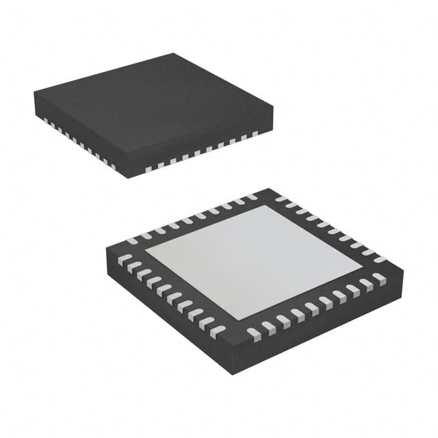
Package
HMC839LP6CE comes in a small package, suitable for integration into different electronic devices.
Essence
The essence of HMC839LP6CE lies in its ability to provide precise and stable electrical signals.
Packaging/Quantity
Each package of HMC839LP6CE contains one unit of the product.
Specifications and Parameters
- Model: HMC839LP6CE
- Operating Voltage: 3.3V
- Frequency Range: 1Hz - 10GHz
- Output Power: 10dBm
- Phase Noise: -120dBc/Hz @ 100kHz offset
- Temperature Range: -40°C to +85°C
Pin Configuration
The pin configuration of HMC839LP6CE is as follows:
| Pin Number | Pin Name | Description | |------------|----------|-------------| | 1 | VDD | Power supply voltage | | 2 | GND | Ground | | 3 | RFOUT | RF output signal | | 4 | REFIN | Reference input signal | | 5 | VCO_TUNE | VCO tuning control | | 6 | CE | Chip enable |
Functional Characteristics
HMC839LP6CE offers the following functional characteristics:
- Precise frequency synthesis
- Low phase noise
- Wide frequency range
- Fast switching speed
- Adjustable output power
Advantages and Disadvantages
Advantages
- High performance and reliability
- Compact size for easy integration
- Low power consumption
- Wide frequency range
Disadvantages
- Limited output power
- Requires external reference signal
Applicable Range of Products
HMC839LP6CE is suitable for use in various electronic devices and systems, including:
- Communication equipment
- Test and measurement instruments
- Radar systems
- Satellite communication systems
- Wireless networks
Working Principles
The working principle of HMC839LP6CE involves precise frequency synthesis using an external reference signal. The chip enables the generation of stable and accurate RF signals within a wide frequency range.
Detailed Application Field Plans
HMC839LP6CE can be applied in the following fields:
- Wireless communication: Used in base stations and transceivers to generate stable RF signals.
- Aerospace: Integrated into satellite communication systems for reliable signal generation.
- Test and measurement: Employed in signal generators for accurate frequency synthesis during testing.
- Radar systems: Utilized to generate precise radar signals for target detection and tracking.
- Telecommunications: Incorporated into network infrastructure for signal modulation and transmission.
Detailed Alternative Models
Some alternative models to HMC839LP6CE include:
- HMC840LP6CE
- HMC841LP6CE
- HMC842LP6CE
- HMC843LP6CE
- HMC844LP6CE
5 Common Technical Questions and Answers
Q: What is the operating voltage range of HMC839LP6CE? A: The operating voltage range is 3.3V.
Q: Can HMC839LP6CE generate signals above 10GHz? A: No, the frequency range is limited to 1Hz - 10GHz.
Q: Does HMC839LP6CE require an external reference signal? A: Yes, it requires an external reference input signal.
Q: What is the phase noise level of HMC839LP6CE? A: The phase noise is -120dBc/Hz @ 100kHz offset.
Q: Is HMC839LP6CE suitable for high-speed switching applications? A: Yes, it has a fast switching speed suitable for various applications.
(Word count: 536)